source:Other information release time:2023-05-12 Hits: Popular:PCB Assembly company

About the original file of pads design
1. PADS paving copper method is the HATCH method paving copper. After the customer's original file is moved, it must be re -paved to save (paved copper with Flood) to avoid short circuit.
2. The hole attributes in the double -panel file PADS must select the pore attribute (Through). You cannot choose the blind buried hole attribute (partial). The drilling file cannot be generated, which will cause the drilling hole.
3. Design slot holes in PADS, please do not add it to the component, because the Gerber cannot be generated normally. To avoid leakage, add grooves to DrillDrawing.
Documents about Protel99se and DXP design
1. The weld is based on the Solder Mask layer. If the sacred layer (Paste layer) needs to be made, there is also a multi -layer (M Ultilayer) welding windows that cannot be generated by GERBER. Please move to the welded layer.
2. Do not lock the outer line in the Protel99se, and you cannot generate a Gerber normally.
3. Do not choose a Keepout option in the DXP file. It will screen outer lines and other components, which cannot generate Gerber.
4. Please pay attention to the front and back design of these two files. In principle, the top layer is positive, and the bottom layer should be designed as an inverse word. Pay special attention to single -piece board, don't mirror at will! It is reversed if it is good.
Read recommendations:
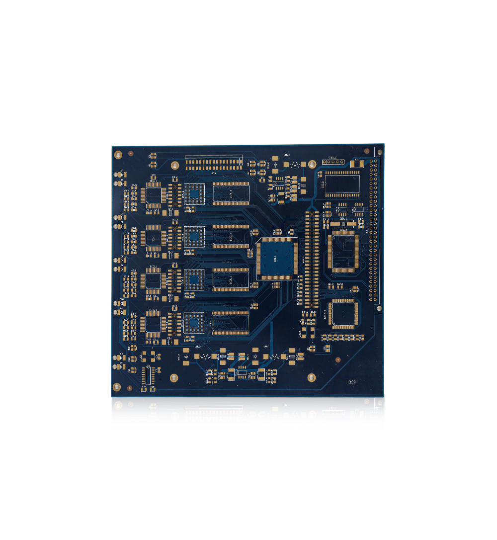
6L 2OZ Multilayer Printed Circuit Board FR4 TG135 Multi Layer Pcb Green Solder Mask
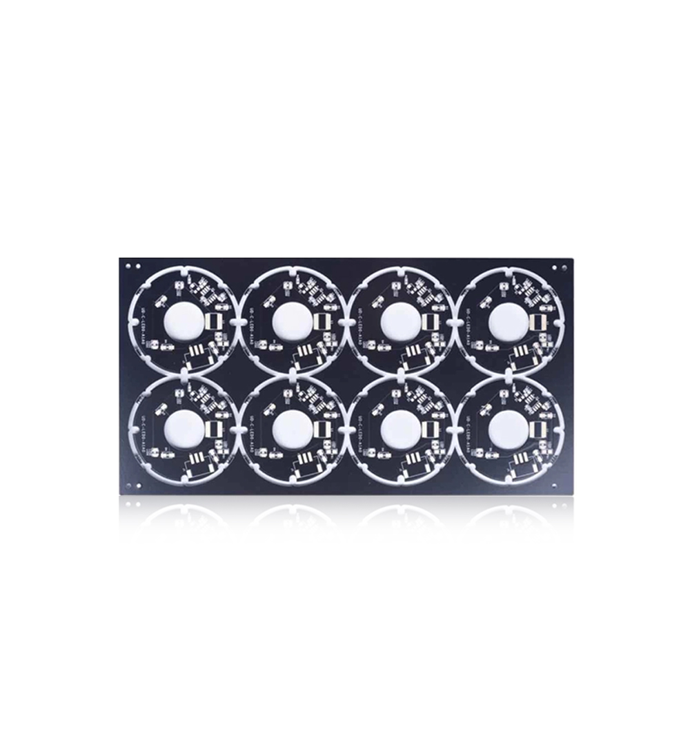
Impedance Control Double Side Prototype PCB 4mil FR4 TG150 Matt Black
Welcome information, we will answer for you quickly

 No. 1 Jingtian Road, Xinsheng community, Longgang District, Shenzhen, Guangdong, China
 +86 13715096176
 Whatsapp/WeChat : +86 13715096176
 Kevin.kuang@xzgcircuits.com


 Return