source:Other information release time:2023-09-08 Hits: Popular:PCB Assembly company

PCB engineers often encounter various safety spacing issues when designing PCBs. These spacing requirements are usually divided into two categories: electrical safety spacing and non electrical safety spacing. So, what are the spacing requirements for designing PCB circuit boards?
1、 Electrical safety spacing
1. Spacing between wires: The minimum distance between wires, also known as line to line and line to pad spacing, should not be less than 4MIL. From a production perspective, under certain conditions, the larger the better. A conventional 10 MIL is relatively common.
2. Pad aperture and pad width: According to the PCB manufacturer's situation, if the pad aperture is mechanically drilled, the minimum should not be less than 0.2mm; If laser drilling is used, the minimum should not be less than 4mil. The aperture tolerance varies slightly depending on the plate, and can generally be controlled within 0.05mm; The minimum width of the welding pad shall not be less than 0.2mm.
3. The spacing between pads: According to the processing capacity of the PCB manufacturer, the spacing should not be less than 0.2MM.
4. The distance between the copper sheet and the edge of the board should preferably not be less than 0.3mm. If copper is laid on a large area, there is usually an internal contraction distance from the edge of the board, usually set at 20mil.
2、 Non electrical safety spacing
1. Character width, height, and spacing: For silk screen characters, conventional values such as 5/30, 6/36 MIL are generally used. Because when the text is too small, it will become blurry when processed and printed.
2. Distance from silk screen to solder pad: silk screen is not allowed to be on the solder pad. Because if the solder pad is covered by the silk screen, the tin cannot be applied to the silk screen during soldering, which affects the installation of components. Generally, PCB manufacturers require a spacing of 8mil to be reserved. If the area of some PCB boards is very tight, achieving a spacing of 4MIL is also acceptable. If the silk screen accidentally covers the solder pad during design, the PCB manufacturer will automatically eliminate the silk screen part left on the solder pad during manufacturing to ensure tin on the solder pad.
3D height and horizontal spacing on mechanical structures: When installing devices on PCBs, it is necessary to consider whether the horizontal direction and spatial height will conflict with other mechanical structures. Therefore, when designing, it is necessary to fully consider the adaptability of the spatial structure between components, as well as between the finished PCB product and the product shell, and reserve safe spacing for each target object.
Read recommendations:
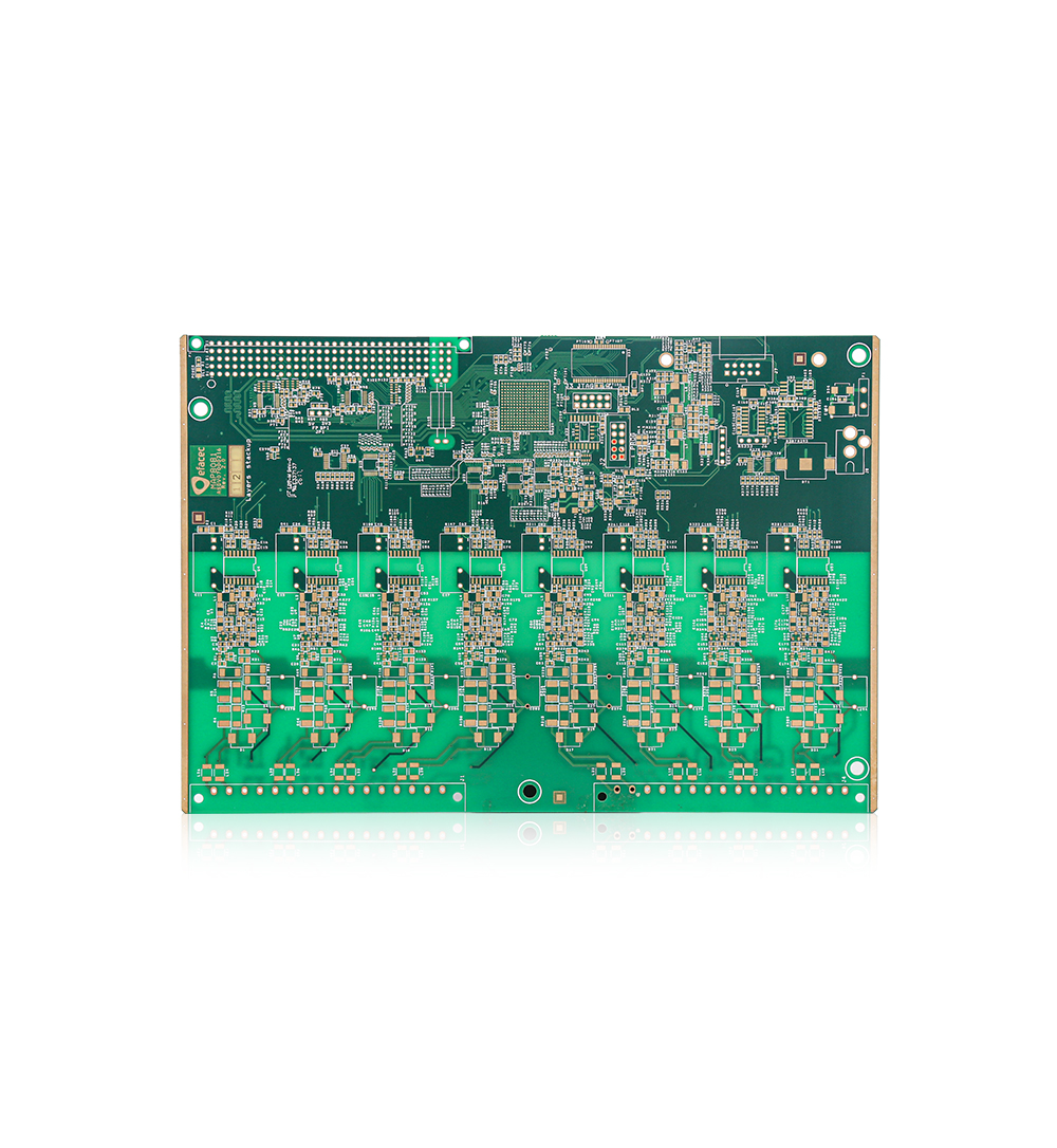
Halogen Free FR4 Multilayer Printed Circuit Board 1.6mm 10mil Impedance Control
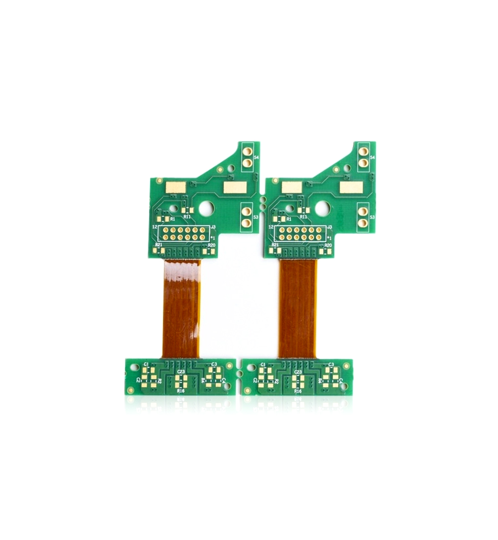
3mil 4L Rigid Flex PCB Black Solder Mask Diy Flexible Circuit Board
Welcome information, we will answer for you quickly

 No. 1 Jingtian Road, Xinsheng community, Longgang District, Shenzhen, Guangdong, China
 +86 13715096176
 Whatsapp/WeChat : +86 13715096176
 Kevin.kuang@xzgcircuits.com


 Return