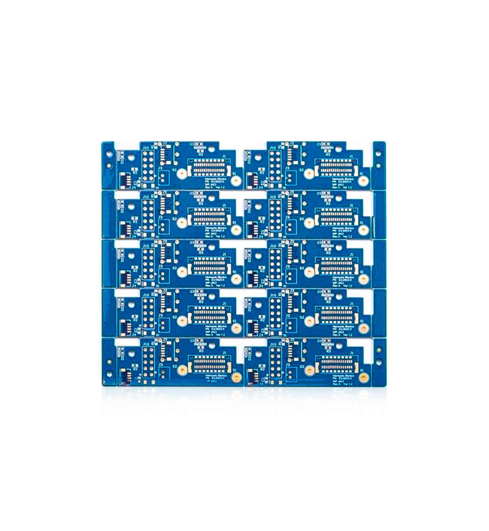
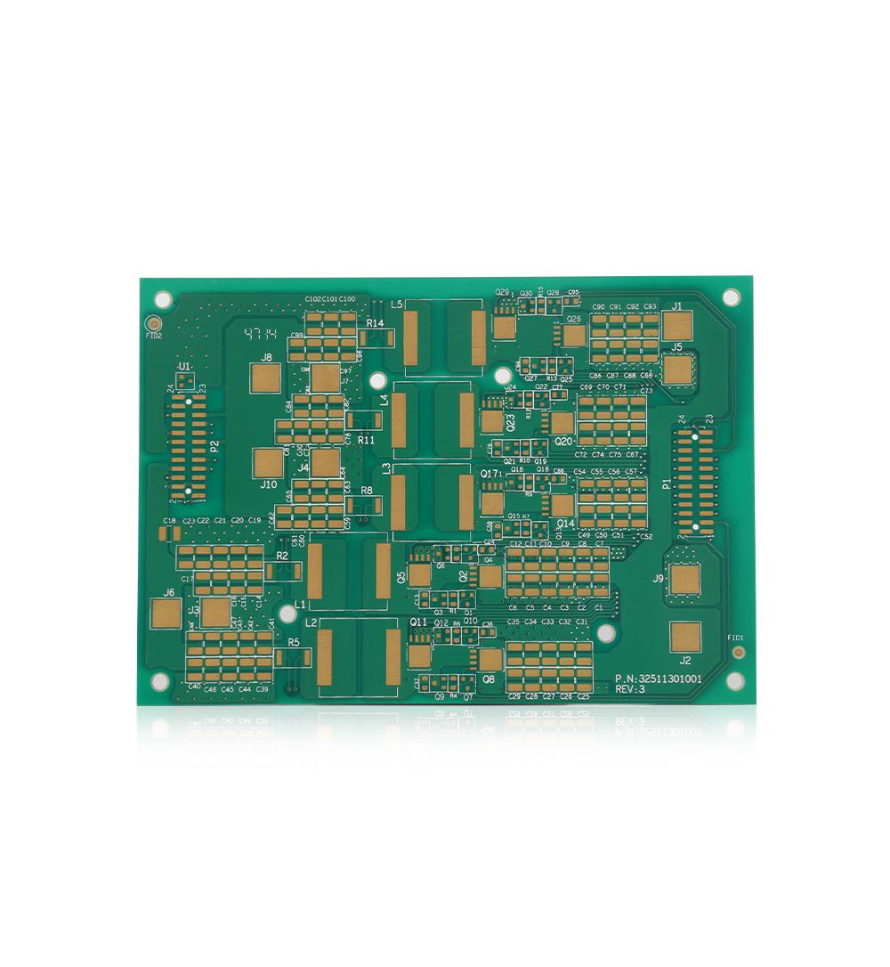
source:Other information release time:2023-05-18 Hits: Popular:PCB Assembly company
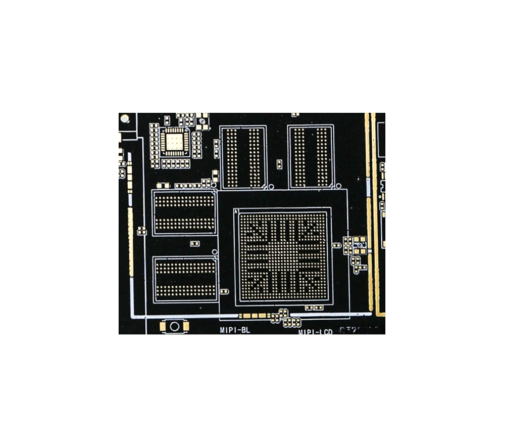
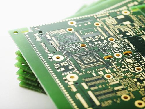
The size of the component on the multi -layer plate is related to the pin size of the selected component. The drilling is too small, which will affect the installation and tin of the device; the drilling holes are too large, and the solder joints are not full enough during welding. Generally speaking, the calculation method of the component hole diameter and the size of the pads is:
The pore diameter of the component hole = component pin diameter (or diagonal line)+(10 ~ 30mil)
Component pad diameter ≥ Componenthole diameter+18mil
As for the pores, the thickness of the finished board is mainly determined by the thickness of the finished board. For high -density and multi -layer boards, it should generally be controlled in the range of the plate thickness: the pore diameter ≤ 5: 1. The calculation method of the pore pad pads is:
Pole pads (ViaPad) diameter ≥ hole diameter+12mil
Read recommendations:
Welcome information, we will answer for you quickly

 No. 1 Jingtian Road, Xinsheng community, Longgang District, Shenzhen, Guangdong, China
 +86 13715096176
 Whatsapp/WeChat : +86 13715096176
 Kevin.kuang@xzgcircuits.com


 Return