source:News release time:2024-01-08 Hits: Popular:PCB Assembly company

The tool for conducting between the components will be designed with a large copper surface as the grounding and power layer. The circuit and the diagram are made simultaneously.
(2) Dielectric layer: Used to maintain the insulation between the circuit and its layers, commonly known as the substrate.
(3) Holes: Through holes can allow two or more layers of circuits to be connected to each other. Larger through holes are used as part inserts, and there are also non through holes, usually used for surface mounting and positioning. They are used to fix screws during assembly.
(4) Solder resistant ink: Not all copper surfaces need to be coated with tin, so areas that are not coated with tin will have a layer of material (usually epoxy resin) printed to isolate the copper surface from tin, avoiding short circuits between non tin coated circuits. The common inks are mainly green oil and blue oil
(5) Screen printing: This is a non essential component, and its main function is to mark the names and location boxes of each component on the circuit board for easy maintenance and identification after assembly.
(6) Surface treatment: Due to the easy oxidation of copper surfaces in general environments, they cannot be soldered (poor solderability), so protection will be applied to the copper surfaces that need to be soldered. The methods of protection include tin spraying, gold plating, silver plating, and tin organic solder flux, each with its own advantages and disadvantages, collectively referred to as surface treatment.
Read recommendations:
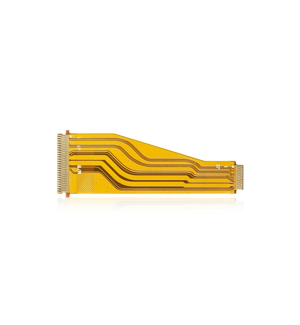
0.8mm Single Layer Rigid Flex PCB Quick Turn 0.5oz Laser Prototyping
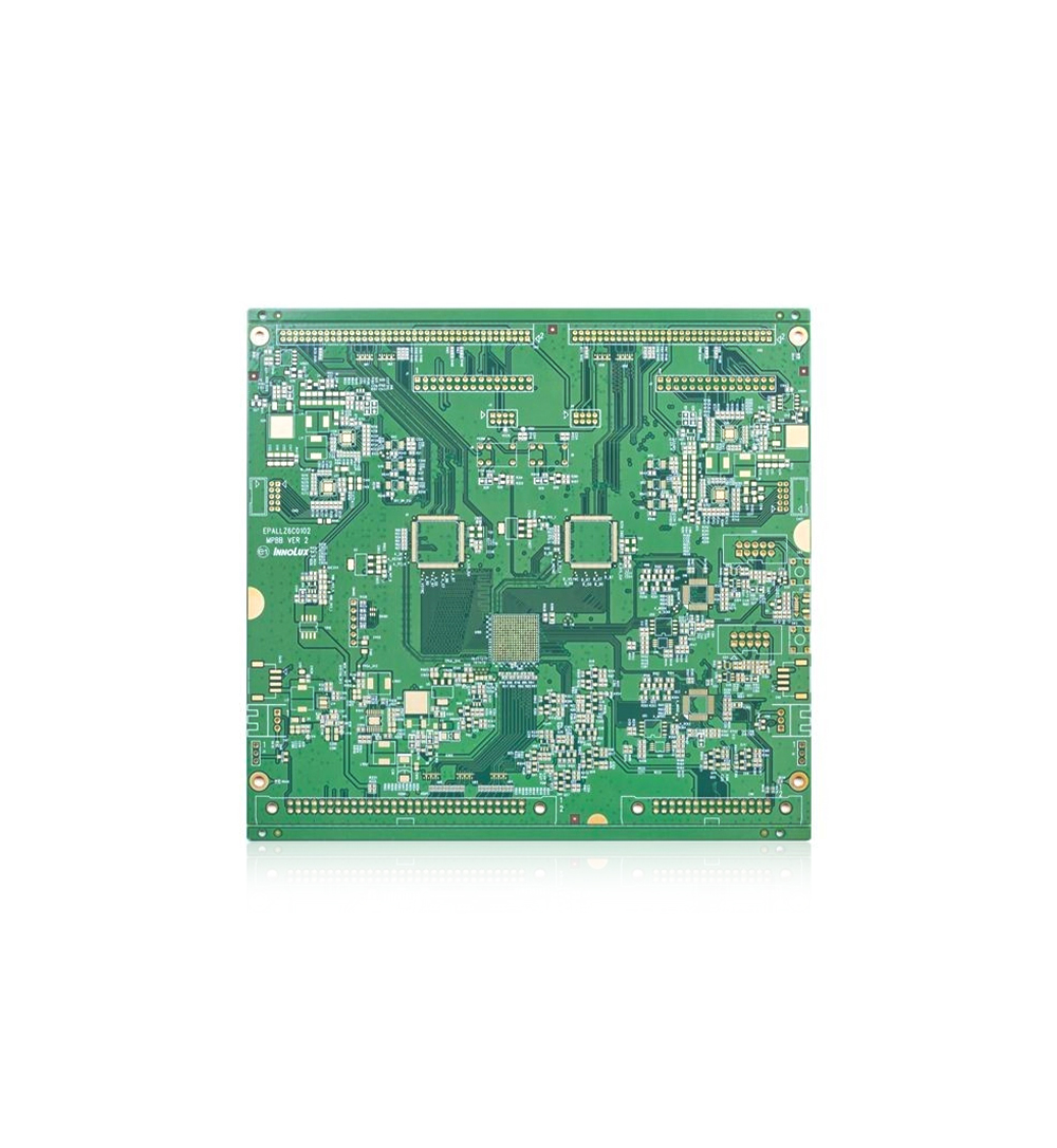
Multilayer Printed Circuit Board
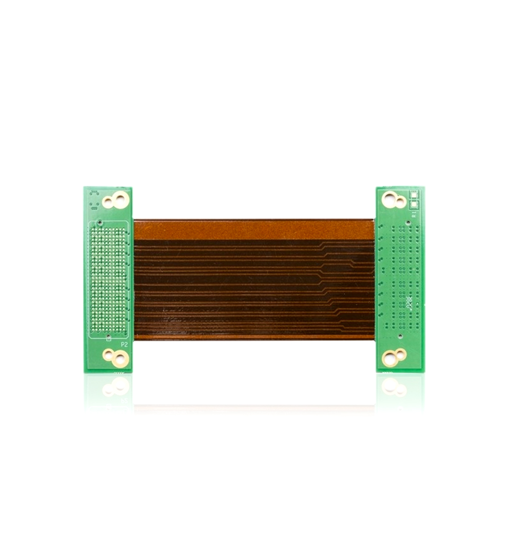
High TG TG170 Double Sided Printed Circuit Board Halogen Free 4mil
Welcome information, we will answer for you quickly

 No. 1 Jingtian Road, Xinsheng community, Longgang District, Shenzhen, Guangdong, China
 +86 13715096176
 Whatsapp/WeChat : +86 13715096176
 Kevin.kuang@xzgcircuits.com


 Return