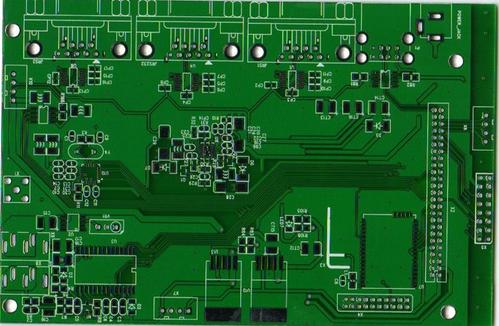
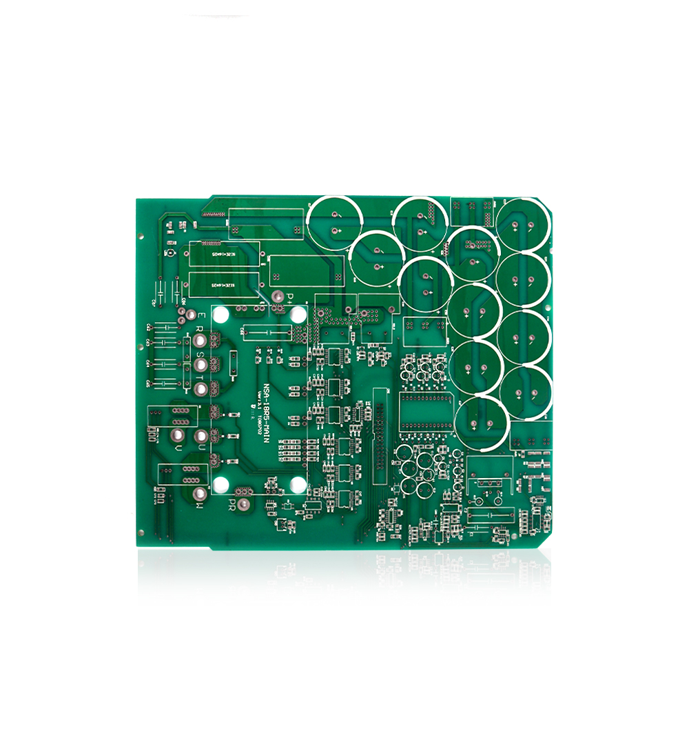
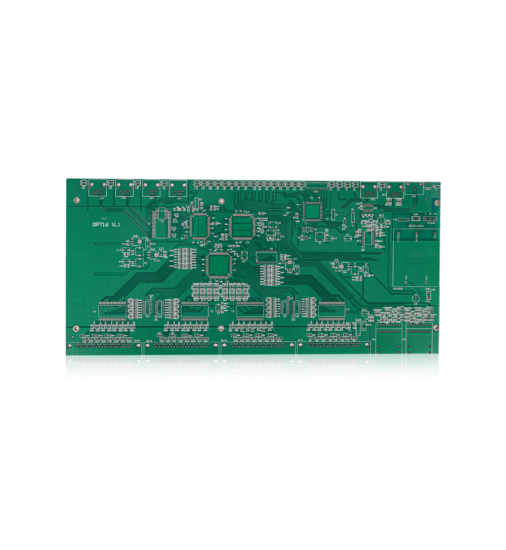
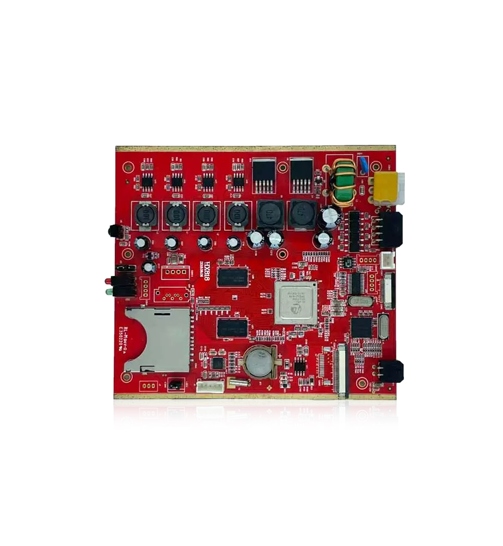
source:Other information release time:2023-04-25 Hits: Popular:PCB Assembly company

Feature impedance: Also known as "feature impedance", it is not a DC resistance, which is the concept of long -term transmission. Within the high frequency range, during the signal transmission process, the signal along, the signal line and the reference plane (power supply or horizon) will generate an instant current due to the establishment of the electric field. If the transmission line is different, then as long as the signal is transmitted, there is always a current I. If the output voltage of the signal is V, during the signal transmission process, the transmission line will be equivalent to a resistor, the size is V/i , Call this equivalent resistor as the characteristic impedance of the transmission line. During the transmission process, if the characteristics of the characteristics on the transmission path change, the signal will reflect on the nodes of the impedance incomplete. The factors that affect the characteristics of characteristic impedance are: dielectric constant, medium thickness, line width, copper foil thickness.
1. Gravity line
Some RF devices are small, and the width of SMD pads may be as small as 12mils, while the RF signal line width may be more than 50mils. The gradient line is used to ban width. The line of the gradient line should not be too long.
2. corner
If the RF signal line goes straight, the effective line width of the corner will increase, and the impedance is not continuous, causing signal reflection. In order to reduce the discontinuousness, there are two ways to deal with the corners: cut corners and rounded corners. The radius of the arc angle should be large enough. Generally speaking, to ensure: R> 3W.
3. Large pad
When there are large pads on the 50 -Euro fine micro -strip line, large pads are equivalent to distributed capacitors, destroying the characteristic impedance continuity of the micro -band line. You can take two methods to improve at the same time: first turn the microstrip medium thicker, and the second plane below the pads can be emptied, which can reduce the distributed capacitors of the pad.
4.
The perforated is a metal cylindrical body plated between the top layer of the circuit board and the bottom layer. The signal over -hole connection is connected to the transmission line at different layers. Pole piles are unused parts of the holes. Pole pads are ring -shaped pads, which connect to the top or internal transmission lines. The isolation disk is a circular gap in each power supply or ground floor to prevent short circuits from the power and ground. If strict physical theory derivation and approximate analysis can be used, the equivalent circuit model of the pores can be connected in series on both ends of the inductance.
It can be seen from the equivalent circuit model that there is a parasitic capacitor to the ground in the perfunction itself. Assuming that the diameter of the over -pores is D2, the diameter of the perforated pads is D1, the thickness of the PCB board is T, and the plate -based dielectric constant is the constant of the plate appliances is the constant of the plate of the board. ε, the parasitic capacitance size of the perforated is similar to:
Pole parasitic capacitors can lead to prolonged signal rising time and slow transmission speed, thereby worsening signal quality. Similarly, there is also a parasitic inductance at the same time. In high -speed digital PCB, the harm of parasitic inductors is often greater than parasitic capacitors.
Read recommendations:
Environmentally Friendly Aluminum PCB Board 1.6mm Single Layer
FR4 1.6mm Double Sided Prototype PCB Board Immersion Gold 4mil
Welcome information, we will answer for you quickly

 No. 1 Jingtian Road, Xinsheng community, Longgang District, Shenzhen, Guangdong, China
 +86 13715096176
 Whatsapp/WeChat : +86 13715096176
 Kevin.kuang@xzgcircuits.com


 Return