source:Other information release time:2023-02-01 Hits: Popular:PCB Assembly company

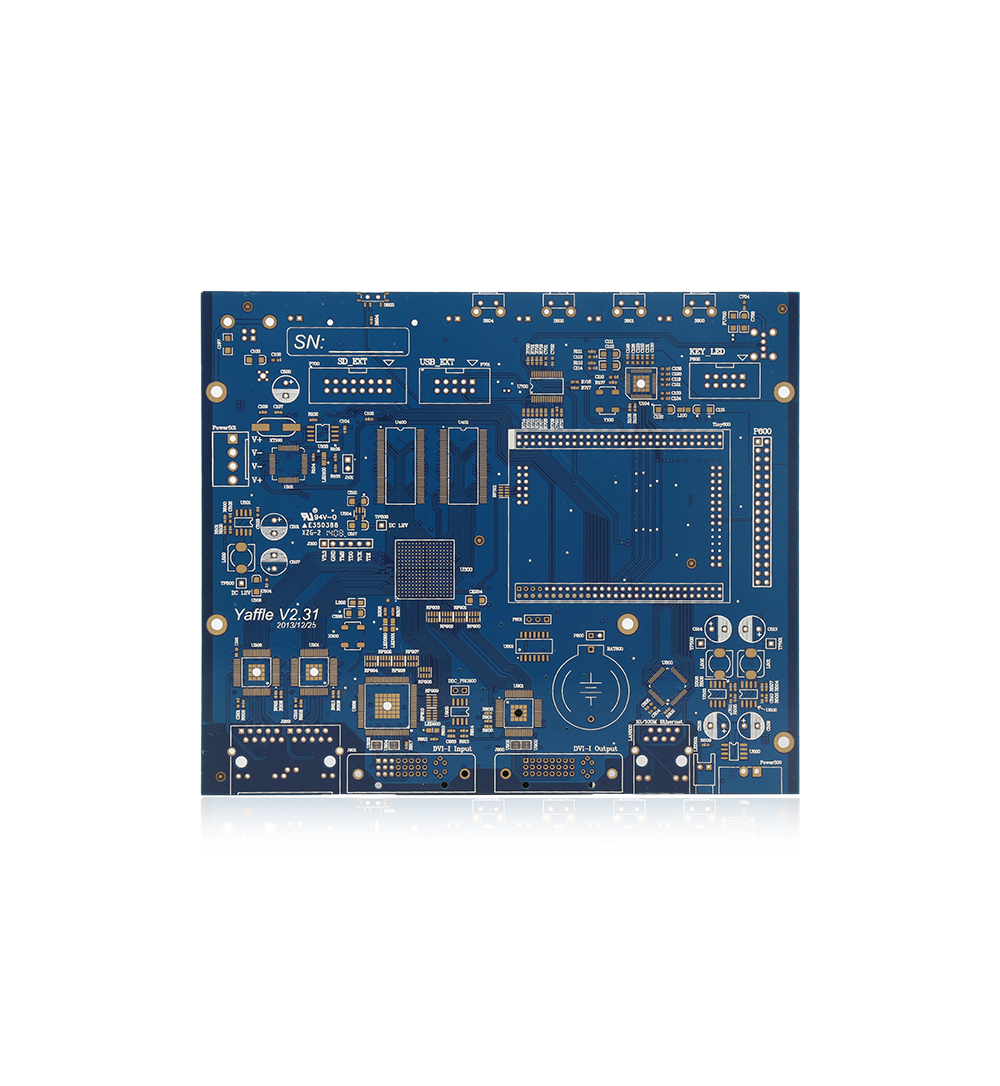
The pad is the basic unit of PCB surface mount assembly. As a PCB design engineer, it is very necessary to understand and master the pad design. Because in the later SMD processing, the quality of the pad design will directly affect the solderability, stability and heat transfer of the components, which is related to the quality of the SMD processing. Next, we might as well understand the design types of the lower pads
Common types of PCB pads
1. Square pads-more used when the printed circuit board components are large and few, and the printed wires are simple. It is easy to use this kind of pads when making a PCB by hand.
aarranged components. If the density of the board allows, the pad can be larger so that it will not fall off during soldering.
3. Island-shaped pad-the connection between the pad and the pad is integrated. It is often used in vertical irregular arrangement installation. For example, such pads are often used in tape recorders.
4. Polygonal pads-used to distinguish pads with close outer diameters but different apertures for easy processing and assembly.
5. Oval pad-This pad has enough area to enhance the anti-stripping ability, and is often used in dual in-line devices.
6. Open-shaped pads-in order to ensure that after wave soldering, the pad holes for manual repair are not sealed by solder.
7. Torx pads—usually used in large vias to ground.
8, cross-pattern pads-also known as thermal pads, hot air pads, etc. Its function is to reduce the heat dissipation of the pad during soldering, so as to prevent false soldering or PCB peeling caused by excessive heat dissipation.
9. Teardrop pad-It is often used when the trace connected to the pad is thin to prevent the pad from peeling and the trace is disconnected from the pad. Such pads are commonly used in high-frequency circuits.
Read recommendations:
Halogen Free FR4 Double Sided PCB 5mil Immersion Gold 1.6mm
Environmentally Friendly Aluminum PCB Board 1.6mm Single Layer
Welcome information, we will answer for you quickly

 No. 1 Jingtian Road, Xinsheng community, Longgang District, Shenzhen, Guangdong, China
 +86 13715096176
 Whatsapp/WeChat : +86 13715096176
 Kevin.kuang@xzgcircuits.com


 Return