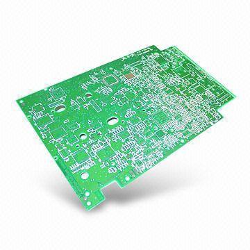
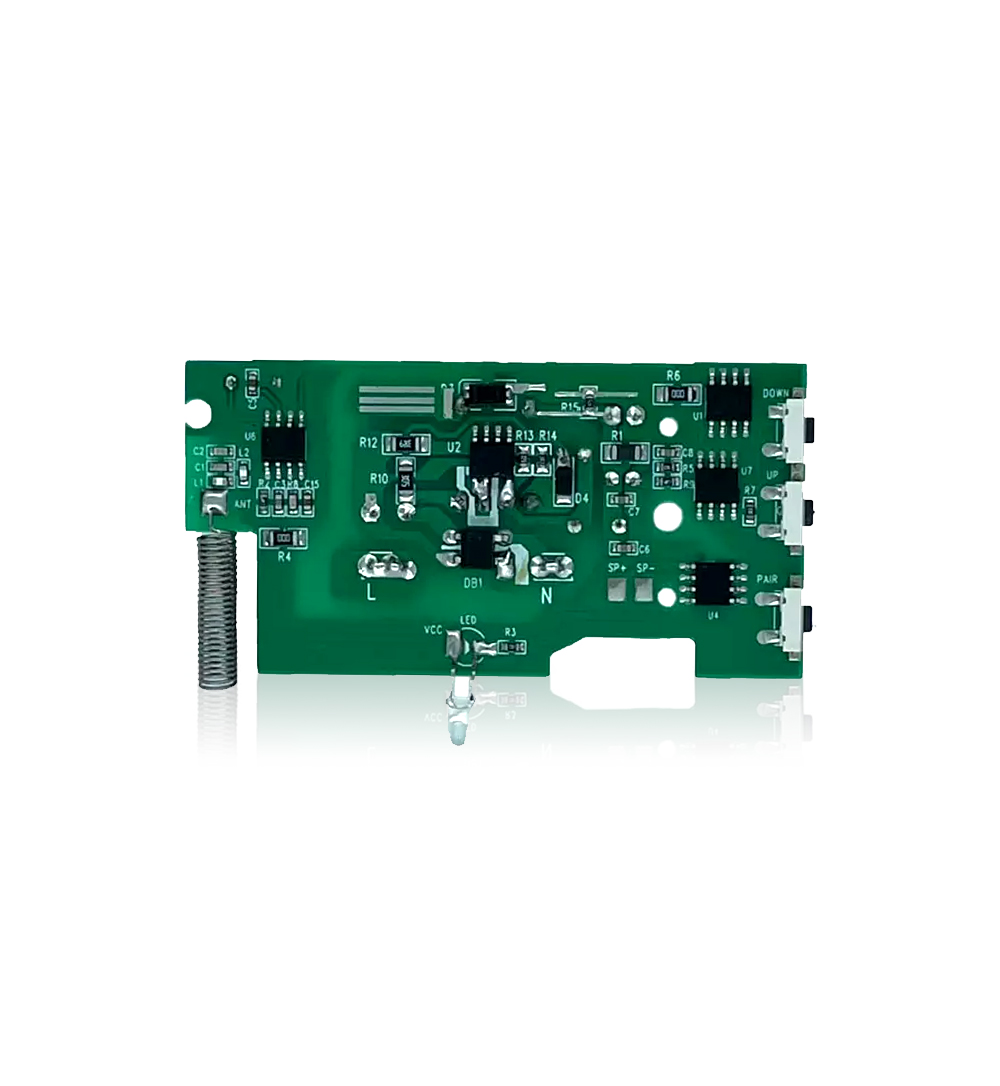
source:News release time:2024-03-15 Hits: Popular:PCB Assembly company

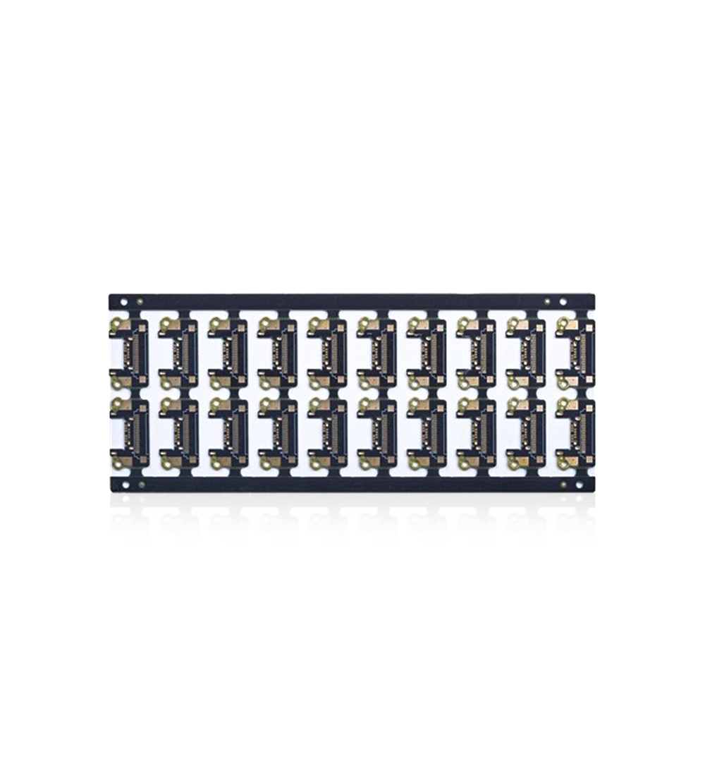
Blind buried hole circuit board: in addition to the completed traditional circuit board, continue to add additional layers successively (Sequent ial); The production of non-machine-drilled micro-blind holes (Microvia, aperture less than 6mi 1) interlayer interconnect, with fine wiring (L/S less than 4mil), and close to the pad (ball pad span less than 30mi 1) of the new layer filler (Sequential Build up; SBU (called HDI (High DensityInterconnect ion) board class, our knowledge of blind buried holes board is very important.
The following three points are made to distinguish the blind buried hole plate:
a: Compared with through holes, through holes refer to holes drilled through all layers, and blind holes are non-drilled through holes.
b: BLIND HOLE subdivision: blind HOLE, BURIED HOLE (the outer layer cannot be seen).
c: Distinguish from the production process: the blind hole is drilled before pressing, and the through hole is drilled after pressing.
So what is the production process of the blind buried hole circuit board?
Open material: The blind hole circuit board needs to choose a better plate, 100% of the 150°C baking plate for 4 hours, to eliminate internal stress and plate moisture.
Drilling: blind hole plate should be careful to use the specified drilling belt, do not misuse, and use a new drill nozzle, stack thickness according to the normal stack thickness of 20%, must ensure that each drilling time, ensure that the associated line is correctly routed. When drilling the inner layer, do not think that the inner layer is thin, it is more laminated, the general requirement is not more than 6PNL, the drilling parameters are 20% slower than the normal parameters, to ensure the quality of the hole wall, no dust and no burrs.
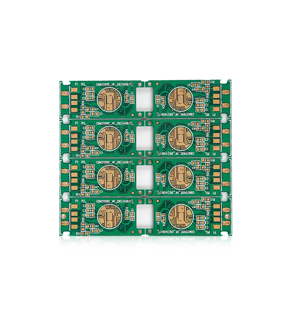
Inner layer: Blind hole plate should pay attention to the identification of direction identification holes, distinguish layers for inner layer production, must not make mistakes in the production of layers, pay special attention to the mirror of each layer, otherwise the correlation relationship of the line will be reversed, and check the film before production, and ensure that the inner line coincidence is intact, the coincidence deviation is less than 0.05mil, and the film should control the expansion coefficient of the film. If the composition is more than 12*12 inches, the film must be enlarged appropriately.
Our blind buried hole circuit board is generally the inner layer in the lateral elongation of 3, 2, vertical elongation, outer horizontal elongation of 5, vertical elongation of 4. This is very important for the production of the follow-up process of the blind hole plate.
https://www.bropool.com/sauna_room/
Read recommendations:
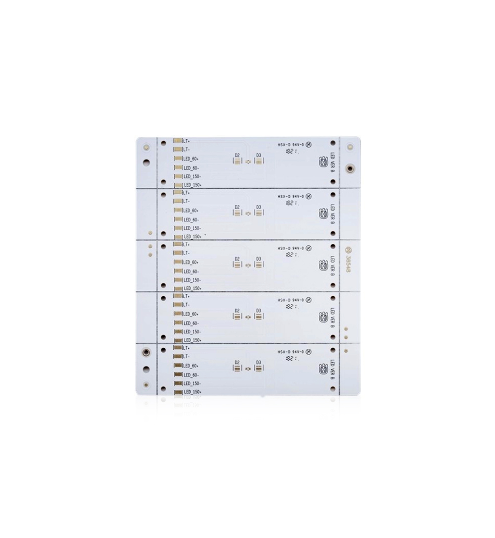
HASL FR4 Single Sided Copper PCB Board White Solder Mask 35um Thickness
Welcome information, we will answer for you quickly

 No. 1 Jingtian Road, Xinsheng community, Longgang District, Shenzhen, Guangdong, China
 +86 13715096176
 Whatsapp/WeChat : +86 13715096176
 Kevin.kuang@xzgcircuits.com


 Return