source:Other information release time:2023-08-02 Hits: Popular:PCB Assembly company

1) In order to reduce the excessive damage of gold to the nickel layer, reduce the occurrence of black pads, and improve the strength of solder joints, the thickness of the gold layer should not exceed 5 inches, and it is best to control it around 3.2 to 3.6 inches.
2) The control of stabilizer should be in accordance with the supplier's regulations. If it exceeds the specifications, there will be skipPlating leakage or edge copper exposure.
3) The temperature and concentration of golden water also play a crucial role. If the temperature is too high and the amount of gold is too small, it will cause excessive corrosion of the nickel layer and the probability of the occurrence of a black pad if the gold layer is covered too slowly or too thin will naturally increase.
4) The condition after gold plating is absolutely important. Any visual uncleanness will result in the powerlessness of the weak soldering flux in the free solder paste. High temperature water flushing, pure water hot washing, ultrasound or air blowing are absolutely necessary. Clean hot air drying is also the key to success or failure.
5) PCB circuit boards for SMT surface welding should not be baked before installation. Baking does not improve the welding performance of the board.
6) Only by reducing the lifespan of the nickel bath to 4MTO and strengthening the management of the gold bath, reducing pollution, or switching to alternative gold plating such as semi replacement and semi reduction.
https://www.bropool.com/hot_tub/
Read recommendations:
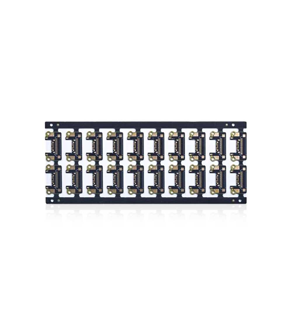
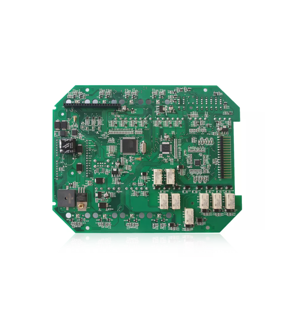
1.6mm FR4 Double Sided Circuit Board Green Solder Mask For Medical Device
PI FR4 Double Layer Flex PCB Board Immersion Gold 2L Lightweight
Welcome information, we will answer for you quickly

 No. 1 Jingtian Road, Xinsheng community, Longgang District, Shenzhen, Guangdong, China
 +86 13715096176
 Whatsapp/WeChat : +86 13715096176
 Kevin.kuang@xzgcircuits.com


 Return