source:Other information release time:2023-05-25 Hits: Popular:PCB Assembly company
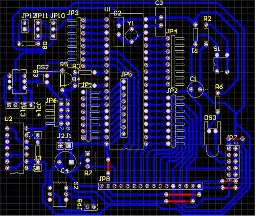
If there is a four -layer board, the components have been removed, and the surface is clean, we must copy it to the PCB file and follow the steps below:
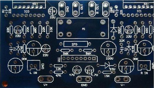
1. Scan the top layer, save the picture, and name top.jpg. At this time, the scanning DPI can be set according to different density. If the settings are 400dpi.
2. Scan the bottom plate, save the picture, and get the name bottom.jpg
3. Make out the middle layer 1 with coarse sandpaper, leak the copper skin, clean it after cleaning, and scan the picture, and get the name MID1.JPG
4. Make the middle layer 2 with coarse sandpaper, leak the copper skin, get it clean, and scan the picture.
5. In the Photoshop, adjust each picture horizontally (select the picture to ensure that the picture is level, so that the lines that come out of this look good, and multiple pictures can be easily aligned). It is recommended to make the underlying image horizontal image in order to make the bottom diagram It is the same direction, the upper and lower positioning holes are the same. Finally, each picture is stored into BMP files, such as: Top.bmp, Bottom.bmp, MID1.BMP, MID2.BMP. It is not necessary to cut the picture just right here. It is best to leave a lot of wealth. Basically, as long as you adjust the picture level, it is over.
Read recommendations:
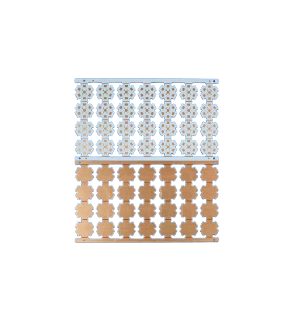
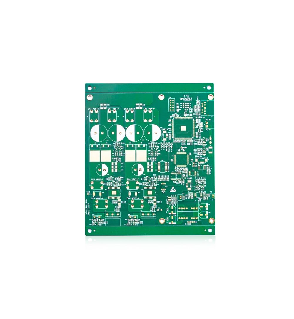
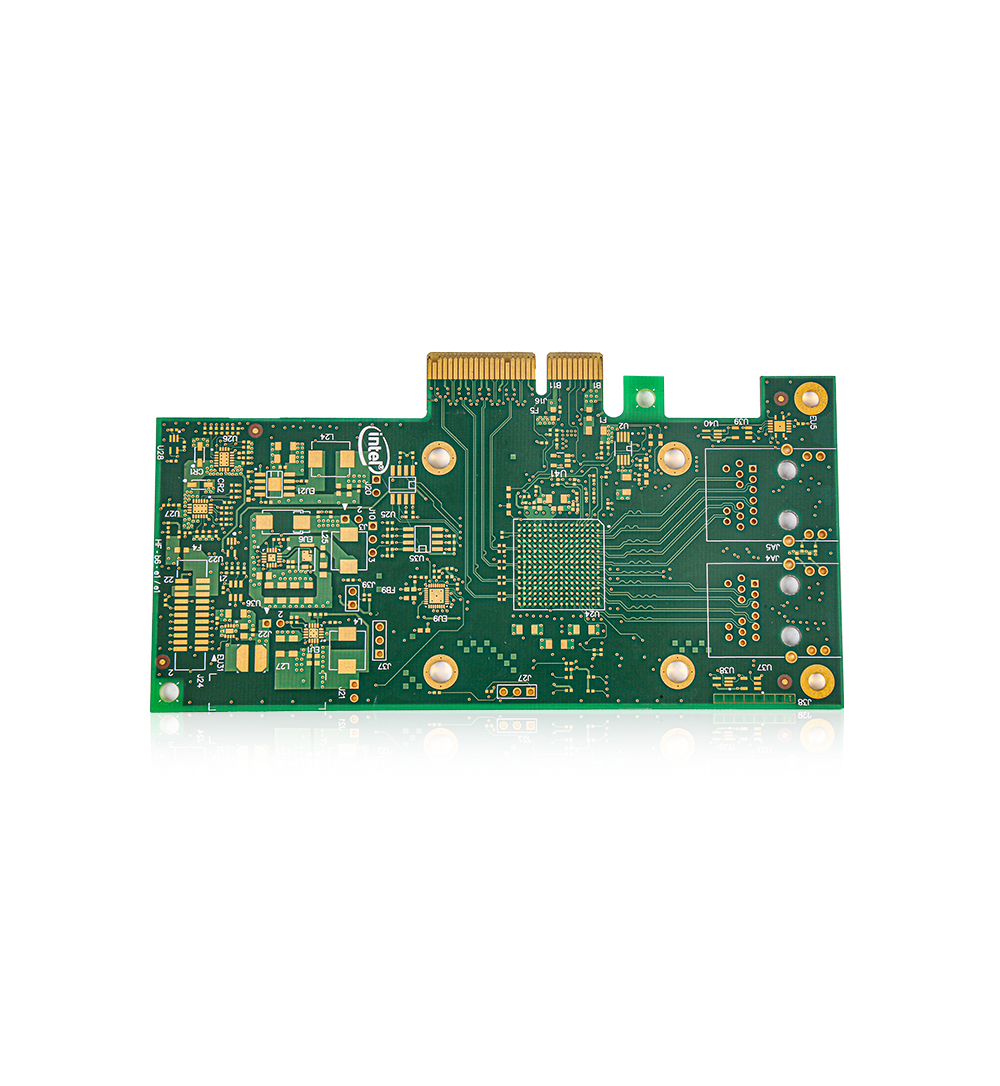
6L 2OZ Multilayer Printed Circuit Board FR4 TG135 Multi Layer Pcb Green Solder Mask
Welcome information, we will answer for you quickly

 No. 1 Jingtian Road, Xinsheng community, Longgang District, Shenzhen, Guangdong, China
 +86 13715096176
 Whatsapp/WeChat : +86 13715096176
 Kevin.kuang@xzgcircuits.com


 Return