source:Other information release time:2023-04-17 Hits: Popular:PCB Assembly company

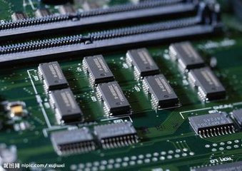
1. The copper surface area on the circuit board is uneven, which will deteriorate the curved board and the plate.
Generally, a large area of copper foil is designed on the circuit board for grounding. Sometimes the VCC layer is also designed with a large area of copper foil. When these large -area copper foils cannot be evenly distributed on the same circuit board, these large -scale copper foil cannot be evenly distributed on the same circuit board. When it is time, the problem of uneven heat absorption and heat dissipation will be caused. Of course, the circuit board will also heat and contraction. If the contraction cannot be reduced at the same time, it will cause different stress and deform. The upper limit of the value will begin to soften, causing permanent deformation.
2. The weight of the circuit board itself will cause the depression of the board
Generally, the welding furnace uses a chain to drive the circuit board to advance in the back welding furnace, that is, to support the entire board as a fulcrum on both sides of the board. If there are too heavy parts on the board, or the size of the board is too large, It will appear in the middle depression because of the amount of itself, causing a curved board.
3. The depth of V-CUT and the connection strip will affect the deformation of the panel
Basically, V-CUT is the culprit that destroys the structure of the board, because V-CUT is to cut the V-shaped groove on a large plate, so the V-CUT place is prone to deformation.
4. The connection points (VIAS) on the circuit board will limit the closure of the board
Most of the current circuit boards are multi -layer boards, and there will be a rivet -like connection point (VIA) between the layers, and the nodes will be divided into pass, blind holes and buried holes. The effect of increased coldness will also indirectly cause plate bending and slab.
Read recommendations:
3mil 4L Rigid Flex PCB Black Solder Mask Diy Flexible Circuit Board
Welcome information, we will answer for you quickly

 No. 1 Jingtian Road, Xinsheng community, Longgang District, Shenzhen, Guangdong, China
 +86 13715096176
 Whatsapp/WeChat : +86 13715096176
 Kevin.kuang@xzgcircuits.com


 Return