source:Other information release time:2022-11-07 Hits: Popular:PCB Assembly company
In addition to the performance of dry film photoresist, the selection of light source, the control of exposure time (exposure amount), and the quality of photographic plate are all important factors affecting the quality of exposure imaging.
1) Selection of light source
Any kind of dry film has its own unique spectral absorption curve, and any kind of light source has its own emission spectral curve. If the main peak of spectral absorption of a certain dry film overlaps or mostly overlaps with the main peak of spectral emission of a certain light source, the two are well matched and the exposure effect is good.
The spectral absorption curve of domestic dry film shows that the spectral absorption range is 310-440 nm (nm). From the spectral energy distribution of several light sources, it can be seen that the pickaxe lamp, high-pressure mercury lamp and iodine gallium lamp have relatively large relative radiation intensity in the wavelength range of 310-440nm, and are ideal light sources for dry film exposure. Xenon lamps are not suitable for exposure to dry film.
After the type of light source is selected, the light source with high power should also be considered. Because of the high light intensity, high resolution and short exposure time, the photographic plate is less deformed by heat. In addition, the design of lamps is also very important. It is necessary to make the incident light as uniform and parallel as possible to avoid or reduce the poor effect after exposure.
2) Control of exposure time (exposure)
In the process of exposure, the photopolymerization of dry film is not "initiated" or "completed in one exposure", but generally goes through three stages.
Due to the presence of oxygen or other harmful impurities in the dry film, an induction process is required. During this process, the free radicals generated from the decomposition of the initiator are consumed by oxygen and impurities, and the polymerization of monomers is very small. However, once the induction period is over, the photopolymerization reaction of monomers will be carried out quickly, and the viscosity of the adhesive film will increase rapidly, close to the degree of mutation. This is the stage of rapid consumption of photosensitive monomers, which accounts for a small proportion of time in the exposure process. When most of the photosensitive monomers are consumed, they enter the monomer depletion zone, and the photopolymerization reaction has been completed.
The correct control of exposure time is a very important factor for obtaining excellent dry film corrosion resistant images. When the exposure is insufficient, due to the incomplete polymerization of monomers, during the development process, the adhesive film swells and becomes soft, the lines are not clear, the color is dim, or even degummed. During the pretreatment or electroplating process, the film is warped, infiltrated, or even peeled off. When the exposure is too high, it will cause problems such as difficult to develop, brittle film, and residual glue. More seriously, incorrect exposure will result in deviation of image line width. Excessive exposure will make the lines of graphic electroplating thinner and the lines of printed etching thicker. On the contrary, insufficient exposure will make the lines of graphic electroplating thicker and the lines of printed etching thinner.
Read recommendations:
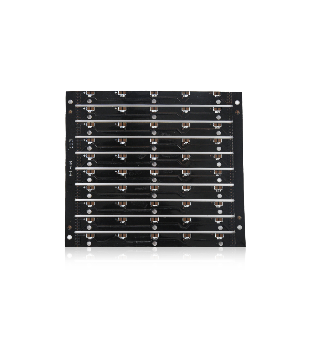
Multilayer Printed Circuit Board
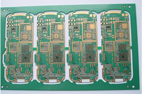
Blue Solder Mask Double Sided PCB Board High TG TG170 S1000-2
Welcome information, we will answer for you quickly

 No. 1 Jingtian Road, Xinsheng community, Longgang District, Shenzhen, Guangdong, China
 +86 13715096176
 Whatsapp/WeChat : +86 13715096176
 Kevin.kuang@xzgcircuits.com


 Return