source:Other information release time:2023-03-29 Hits: Popular:PCB Assembly company

You can understand the characteristics of selective welding by comparison with the peak welding. The most obvious difference between the two is that the lower part of the PCB in the peak welding is completely immersed in liquid solder, and in selective welding, only some specific areas are in contact with weld waves. Because PCB itself is a bad thermal conductivity, it does not heat the melt -melting neighboring component and PCB area welding joints during welding. Before welding, you must also apply the welding pre -welding. Compared with wave welding, the welded agent only coated at the lower part of the welding part of the lower part of the PCB, not the entire PCB. In addition, selective welding is only suitable for welding of inserted elements. Selective welding is a new method that thoroughly understands that selective welding processes and equipment are necessary for successful welding.
Welding coating process
In selective welding, the coating process of the welded agent plays an important role. At the end of welding heating and welding, the welded agent should have sufficient activity to prevent bridges from generating and prevent PCB from oxidizing. The welding spray was carried by the X/Y robotic hand to carry the PCB above the top of the welded nozzle, and the welded agent was sprayed on the PCB to the welding position. The welds have a single -mouth spray type, microporous jet type, synchronous multi -point/graphic spray. The microwave peak selected welding after the return welding process is the most important thing is to accurately spray the welds. Micro -hole jet type will definitely not stain the area outside the welding joint. The diameter of the minimum welding point of the micro -point spray is greater than 2mm, so the location accuracy of the welding deployed on the PCB is ± 0.5mm to ensure that the solder is always covered on the welded area. The amount of welded doses is generally recommended for 100%safety tolerance range.
Preheating process
The main purpose of the preheating in selective welding process is not to reduce thermal stress, but to remove solvents pre -drying welds. Before entering the welding wave, the solder has the correct viscosity. When welding, the effect of the heat in the preheating on the welding quality is not a key factor. The thickness of the PCB material, the equipment packaging specifications and the type of welding agent determine the preheating temperature. In selective welding, there is a different theoretical explanation of preheating: Some process engineers believe that PCB should be preheated before the welding agent is sprayed; another point of view is that the welding does not need to be preheated and directly welded. Users can arrange selective welding processes based on specific conditions.
Welding process
There are two different processes in selective welding processes: drag welding process and leaking technology.
Selective welding process is completed on a single small welding welding wave. Welding technology is suitable for welding on a very close space on PCB. For example: individual welded joints or pins, single rows of feet can perform a mop welding process. PCB moves the best welding quality on the welded welding wave at different speeds and angles. To ensure the stability of the welding process, the inner diameter of the welding mouth is less than 6mm. After the direction of the welding solution is determined, it is installed and optimized in different directions for different welding needs. The robot can be close to weld waves from different angles between different directions, that is, 0 degrees, that is, 0 degrees, that is, 0 degrees, between 0 degrees and 12 degrees, so users can weld various devices on electronic components. For most devices, it is recommended to lean angle at 10 degrees.
Read recommendations:
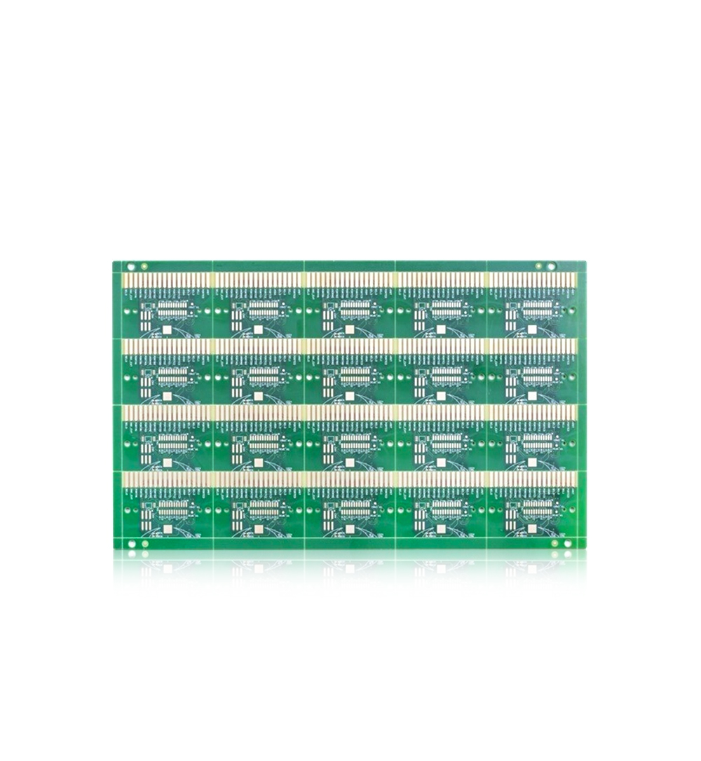
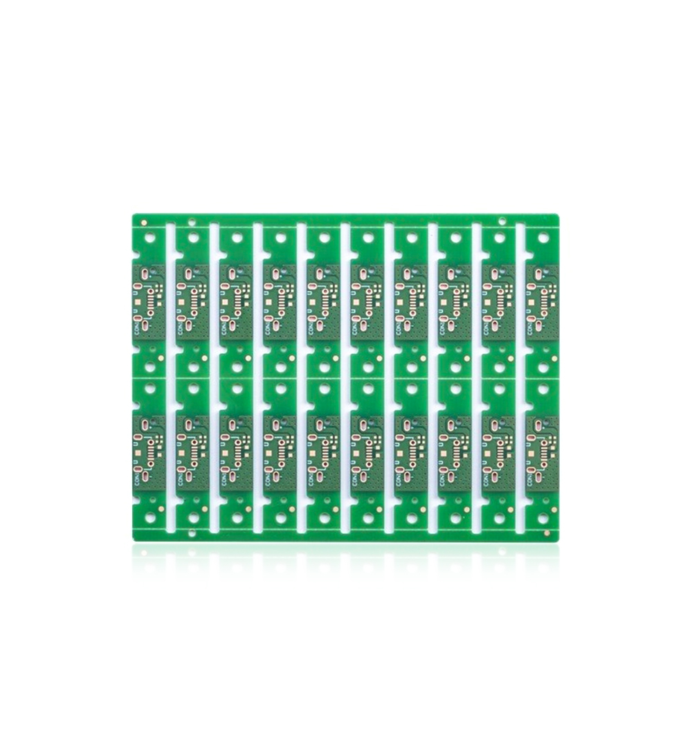
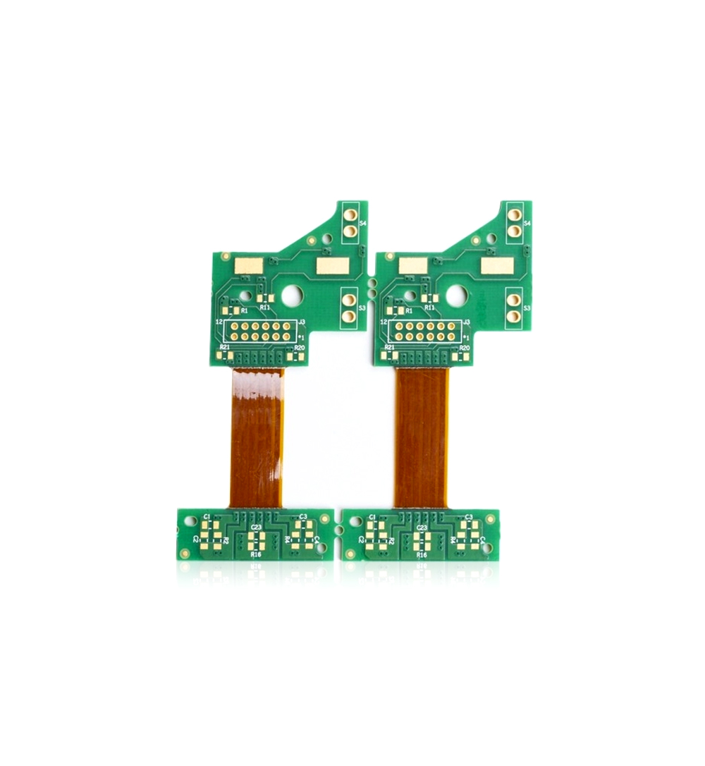
1.5oz Multilayer Pcb Fabrication FR4 Printed Circuit Board Pcb 4 Layer
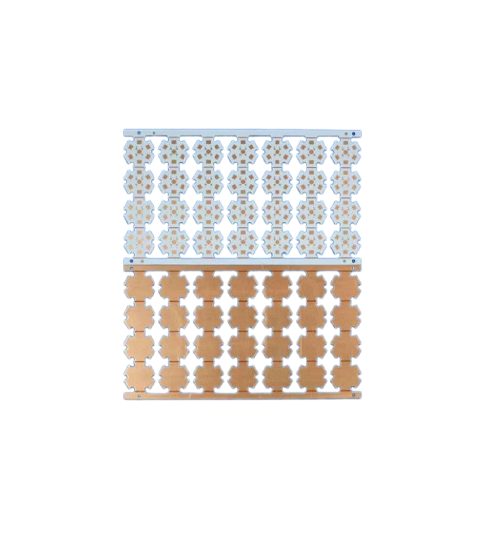
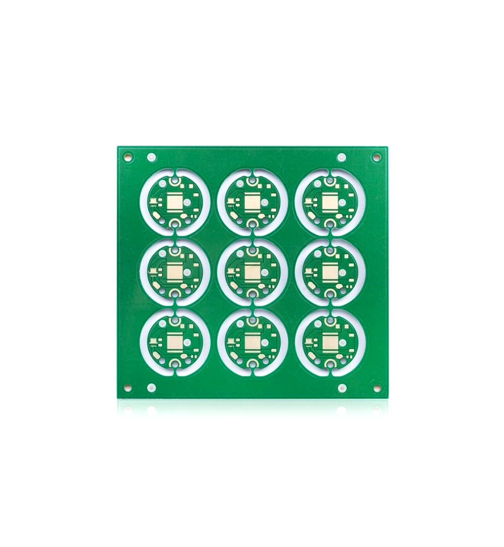
Lightweight Aluminum PCB Board Green Solder Mask Led Light Pcb Board 3.0mm
Welcome information, we will answer for you quickly

 No. 1 Jingtian Road, Xinsheng community, Longgang District, Shenzhen, Guangdong, China
 +86 13715096176
 Whatsapp/WeChat : +86 13715096176
 Kevin.kuang@xzgcircuits.com


 Return