source:News release time:2023-07-07 Hits: Popular:PCB Assembly company

Before packaging, conduct the final electrical conduction, impedance test, solderability and Thermal shock resistance test on the circuit board. And use moderate baking to eliminate the moisture and accumulated thermal stress absorbed by the circuit board during the manufacturing process, and finally use vacuum bags to package and ship.
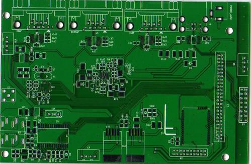
In recent years, with the development of miniaturization and high integration of VLSI and electronic components, multi-layer boards have mostly moved towards the direction of matching with high-performance circuits. As a result, there is an increasing demand for high-density circuits and high wiring capacity, and also a stricter requirement for electrical characteristics (such as the integration of Crosstalk and impedance characteristics). The prevalence of multi pin components and surface mount devices (SMD) has led to more complex shapes of circuit board patterns, smaller conductor lines and apertures, and the development of higher multilayer boards (10-15 layers) has become a trend. In the latter half of the 1980s, in order to meet the needs of small and lightweight high-density wiring and small hole trends, thin multilayer boards with a thickness of 0.4~0.6 mm gradually became popular. Complete the guide hole and shape of the part through punching processing. In addition, some products produced in small quantities and in various forms are photographed using photosensitive agents to form patterns.
High power amplifier base material: ceramic+FR-4 plate+copper base, number of layers: 4 layers+copper base, surface treatment: gold deposition, characteristics: ceramic+FR-4 plate mixed lamination, copper base bonding
Military high-frequency multi-layer board - substrate: PTFE, plate thickness: 3.85mm, number of layers: 4, features: blind buried holes, silver slurry filled holes
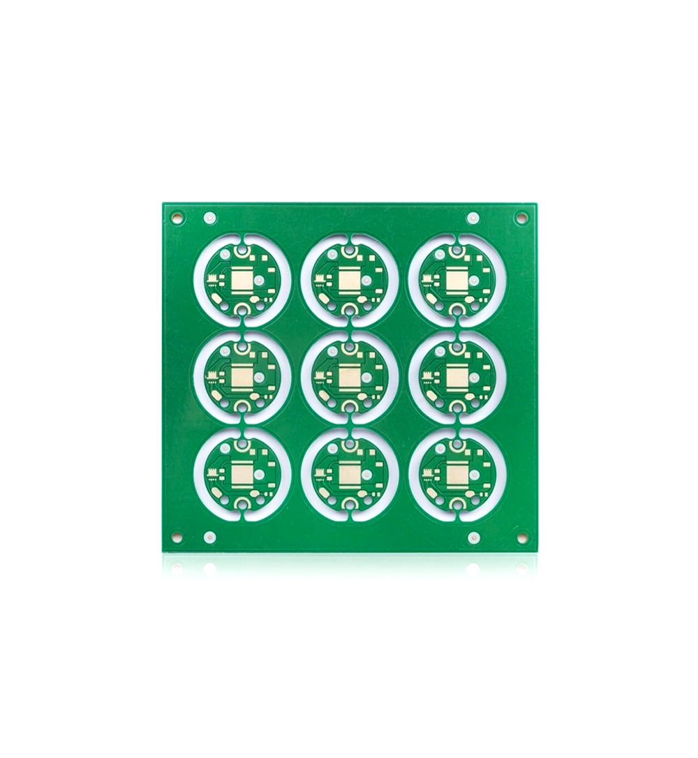
Green product - substrate: environmentally friendly FR-4 board, board thickness: 0.8mm, number of layers: 4, size: 50mm × 203mm, line width/line spacing: 0.8mm, aperture: 0.3mm, surface treatment: sinking gold and tin
High frequency and high Tg devices - substrate: BT, number of layers: 4, plate thickness: 1.0mm, surface treatment: gold plating
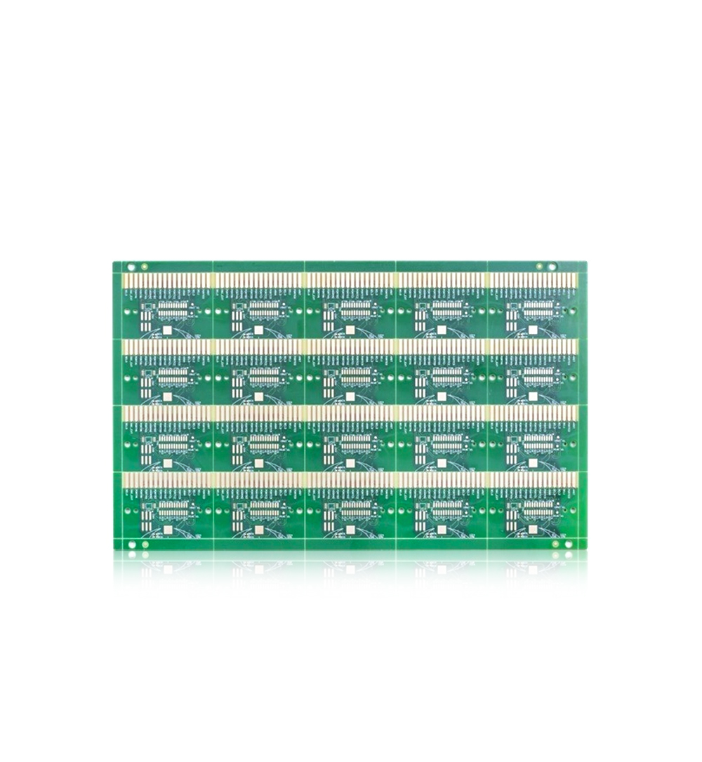
Embedded system - substrate: FR-4, number of layers: 8, plate thickness: 1.6mm, surface treatment: tin spraying, line width/line spacing: 4mils/4mils, solder mask color: yellow
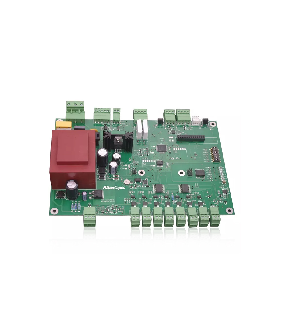
DCDC, power module - substrate: high Tg thick copper foil, FR-4 sheet, size: 58mm × 60mm, line width/line spacing: 0.15mm, aperture: 0.15mm, plate thickness: 1.6mm, number of layers: 10, surface treatment: gold deposit, features: copper foil thickness of 3OZ (105um) per layer, blind buried hole technology, high current output
Read recommendations:
Polymer Film Flex PCB Board 0.1mm 2 Layer Rigid Flex Pcb Lightweight
3mil 4L Rigid Flex PCB Black Solder Mask Diy Flexible Circuit Board
Impedance Control Double Side Prototype PCB 4mil FR4 TG150 Matt Black
Welcome information, we will answer for you quickly

 No. 1 Jingtian Road, Xinsheng community, Longgang District, Shenzhen, Guangdong, China
 +86 13715096176
 Whatsapp/WeChat : +86 13715096176
 Kevin.kuang@xzgcircuits.com


 Return