source:Other information release time:2023-05-06 Hits: Popular:PCB Assembly company
1、 Establish component parameters from schematic diagram to PCB design process ->Input schematic network table ->Design parameter settings ->Manual layout ->Manual wiring ->Validate design ->Review ->CAM output.
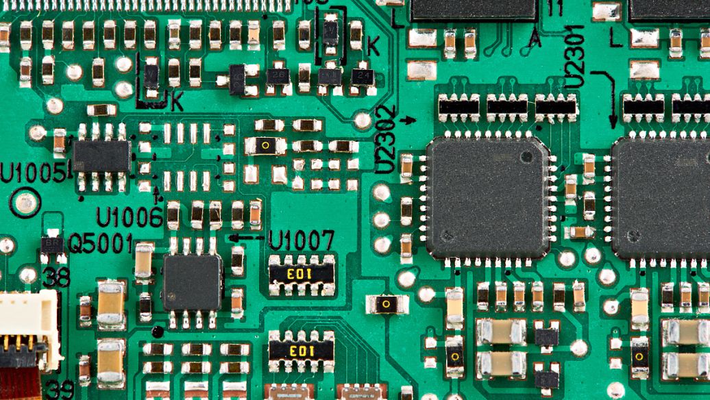
2、 The spacing between adjacent conductors in parameter setting must meet the requirements of Electrical safety, and in order to facilitate operation and production, the spacing should also be as wide as possible. The minimum spacing should be at least suitable for the voltage it can withstand. When the wiring density is low, the spacing between signal lines can be appropriately increased. For signal lines with significant differences between high and low levels, the spacing should be as short and increased as possible. Generally, the wiring spacing should be set to 8mil
The distance from the edge of the inner hole of the solder pad to the edge of the printed board should be greater than 1mm, which can avoid causing solder pad defects during processing. When the wiring connected to the pad is thin, the connection between the pad and the wiring should be designed as a water droplet shape. This has the advantage that the pad is not easy to peel, and the wiring is not easily disconnected from the pad.
3、 The practice of component layout has proven that even if the circuit schematic design is correct and the printed circuit board design is inappropriate, it can have a negative impact on the reliability of electronic equipment. For example, if two thin parallel lines of a printed circuit board are close together, it will cause a delay in the signal waveform and generate reflected noise at the end of the transmission line; The interference caused by inadequate consideration of power and ground wires can lead to a decrease in product performance. Therefore, when designing printed circuit boards, attention should be paid to using the correct methods. Each switching power supply has four current circuits:
(1) Power switch AC circuit
(2) Output rectifier AC circuit
Read recommendations:
Immersion Gold IPC Class 3 PCB Double Sided Green Solder Mask 4mil 1.6mm
Welcome information, we will answer for you quickly

 No. 1 Jingtian Road, Xinsheng community, Longgang District, Shenzhen, Guangdong, China
 +86 13715096176
 Whatsapp/WeChat : +86 13715096176
 Kevin.kuang@xzgcircuits.com


 Return