source:Other information release time:2023-08-10 Hits: Popular:PCB Assembly company

Next, the editor will tell you the difference between PCB board making and sampling. I hope this article can help you.
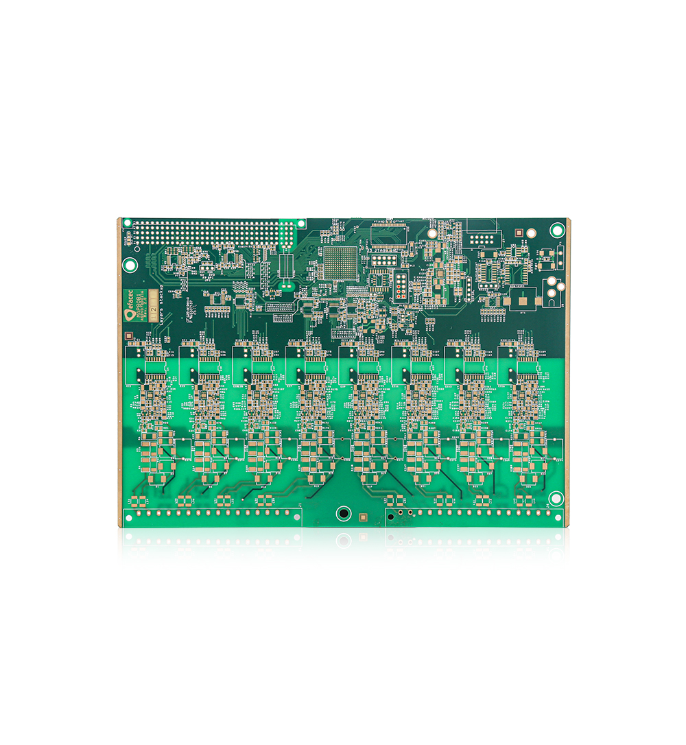
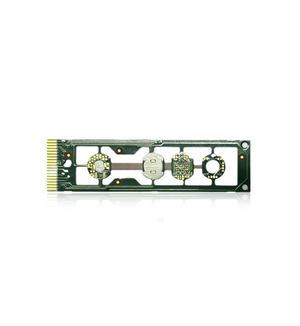
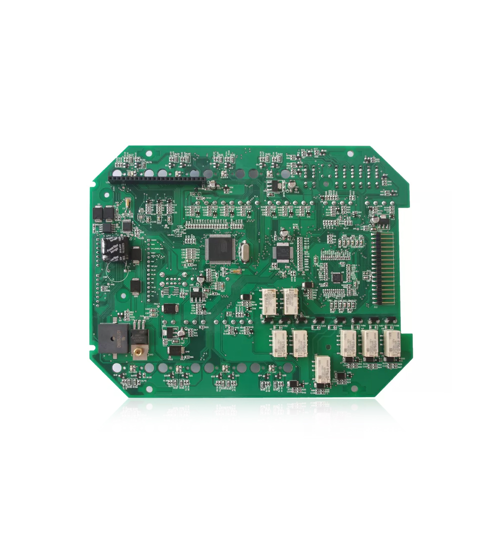
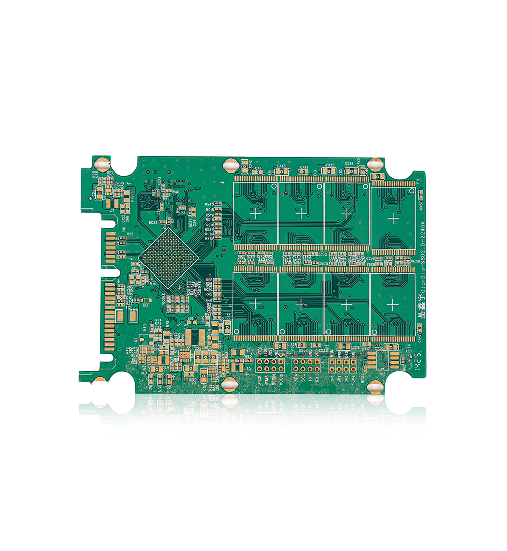
Usually, PCB engineers will draw PCB structural diagrams according to the different specifications and requirements of customers. The main structural layers can be divided into single-sided, double-sided, and multi-layer circuit boards.
Based on the circuit board diagram drawn by the PCB engineer, sample making is commonly referred to as PCB sampling.
The specific process for PCB sampling is as follows:
Firstly, we need to inform the manufacturer of the required size, process requirements, product quantity, and other relevant data. Then, professional personnel will provide you with a quotation, place an order, and follow up on the production situation.
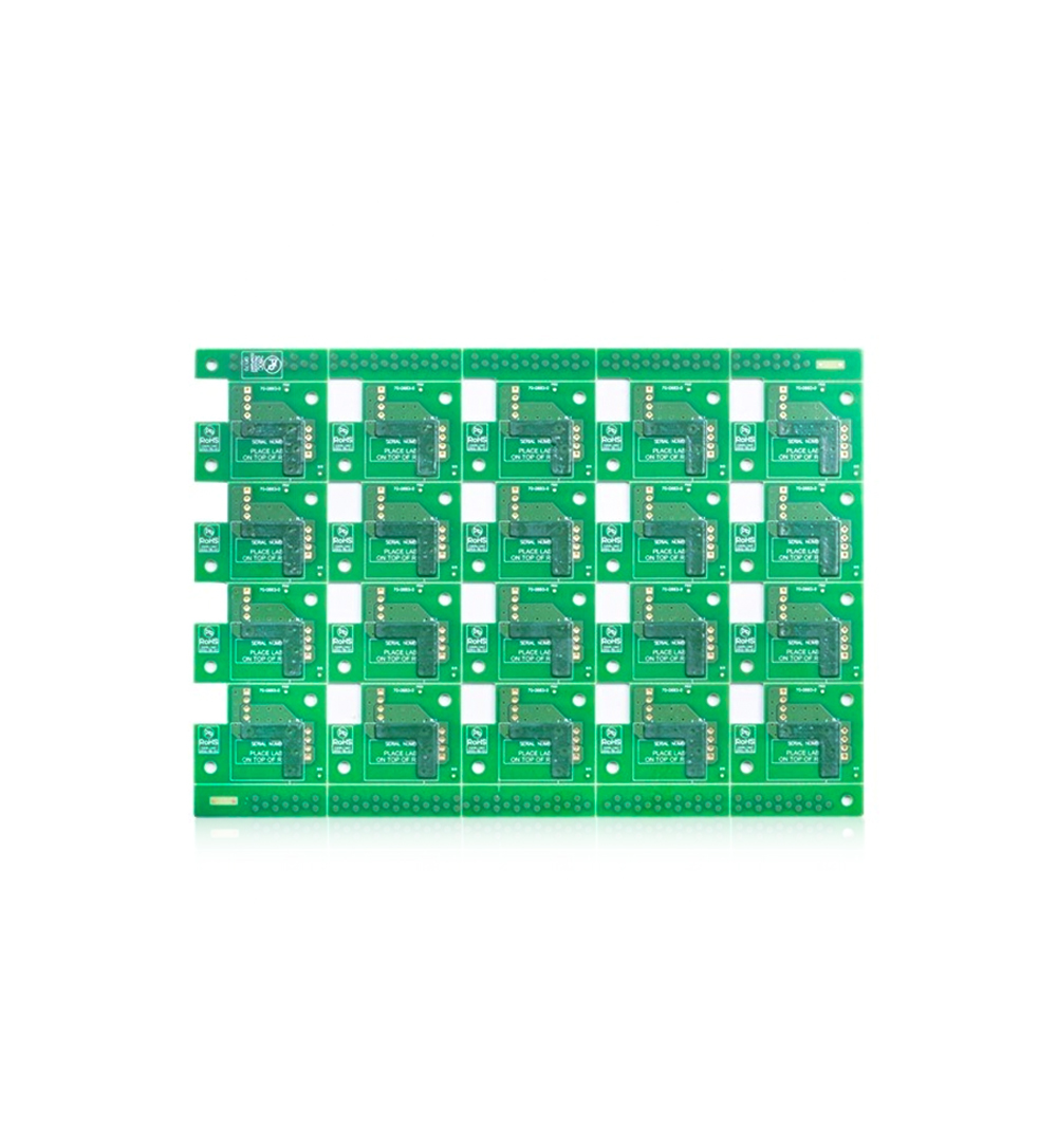
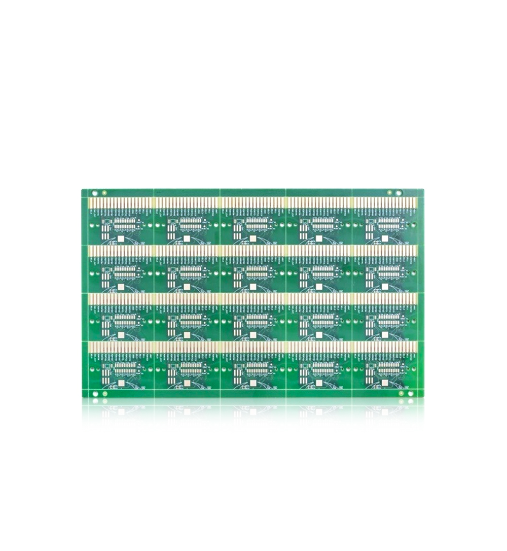
According to the customer's requirements, cut small pieces of production boards that meet the requirements on the board. The specific process is as follows: large board material → cutting according to MI requirements → cutting board → cutting board → rounding/grinding edge → discharging board.
The main operation is to drill holes according to the customer's information, and drill the required hole size at the appropriate position. The specific process is as follows: stack pin → upper plate → drilling → lower plate → inspection/repair.
The main operation is copper deposition. The principle of copper deposition is to use chemical methods to deposit a thin layer of copper on the insulation hole. The specific process is as follows: rough grinding → hanging board → automatic copper deposition line → bottom board → immersion in 1% dilute H2SO4 → thickening of copper.
Read recommendations:
1OZ 1.0mm Aluminum PCB Board OSP Finished Aluminium Substrate Pcb
Immersion Gold 4 Layer Flex Pcb Rigid Printed Circuit Board 2.0mm 3mil
Welcome information, we will answer for you quickly

 No. 1 Jingtian Road, Xinsheng community, Longgang District, Shenzhen, Guangdong, China
 +86 13715096176
 Whatsapp/WeChat : +86 13715096176
 Kevin.kuang@xzgcircuits.com


 Return