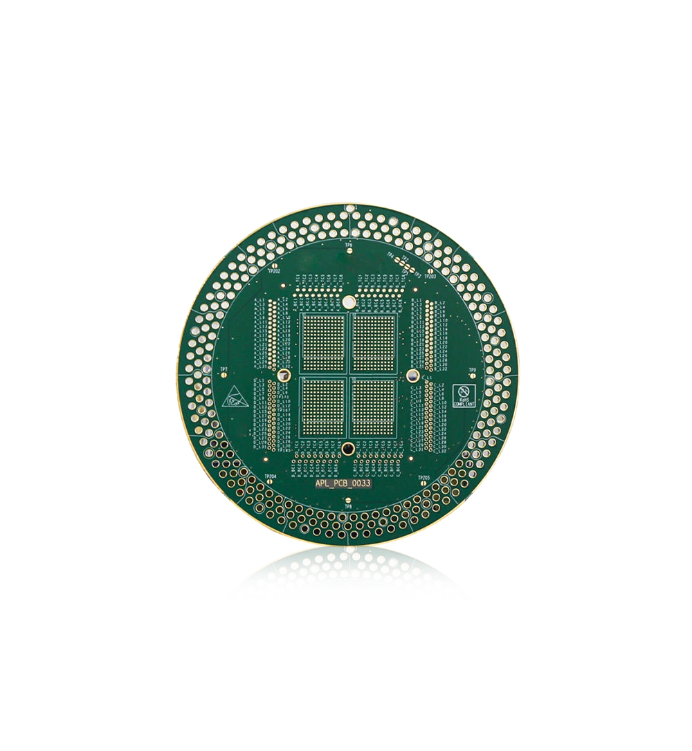
source:News release time:2023-04-21 Hits: Popular:PCB Assembly company

The welded layer is used for patch packaging and corresponds to pad pad pads. A steel plate is usually used during SMT processing, and the PCB corresponds to the place where the component pads corresponding to the component pad, and then the steel plate is put on the tin paste. When the PCB is under the steel plate, the tin paste is leaked, and it just happens to be on each pad on each pad. It can be stained with solder, so the welding layer is usually not greater than the actual pad size. It is best to be less than or equal to the actual pad size.
The required levels are almost the same as the table stickers, and the main elements are mainly required: the following:
1. Beginlayer: ThermalRelief and Antipad are 0.5mm larger than the actual size of the regular pad
2. EndLayer: Thermalrelief and antiPad are 0.5mm larger than the actual size of the regular pad
3. DEFAULTINTERNAL: middle layer
Read recommendations:
Halogen Free FR4 Multilayer Printed Circuit Board 1.6mm 10mil Impedance Control
Welcome information, we will answer for you quickly

 No. 1 Jingtian Road, Xinsheng community, Longgang District, Shenzhen, Guangdong, China
 +86 13715096176
 Whatsapp/WeChat : +86 13715096176
 Kevin.kuang@xzgcircuits.com


 Return