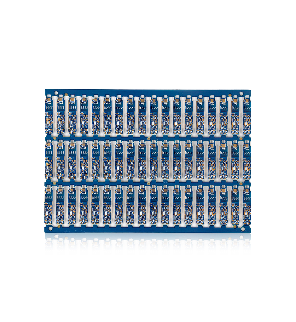
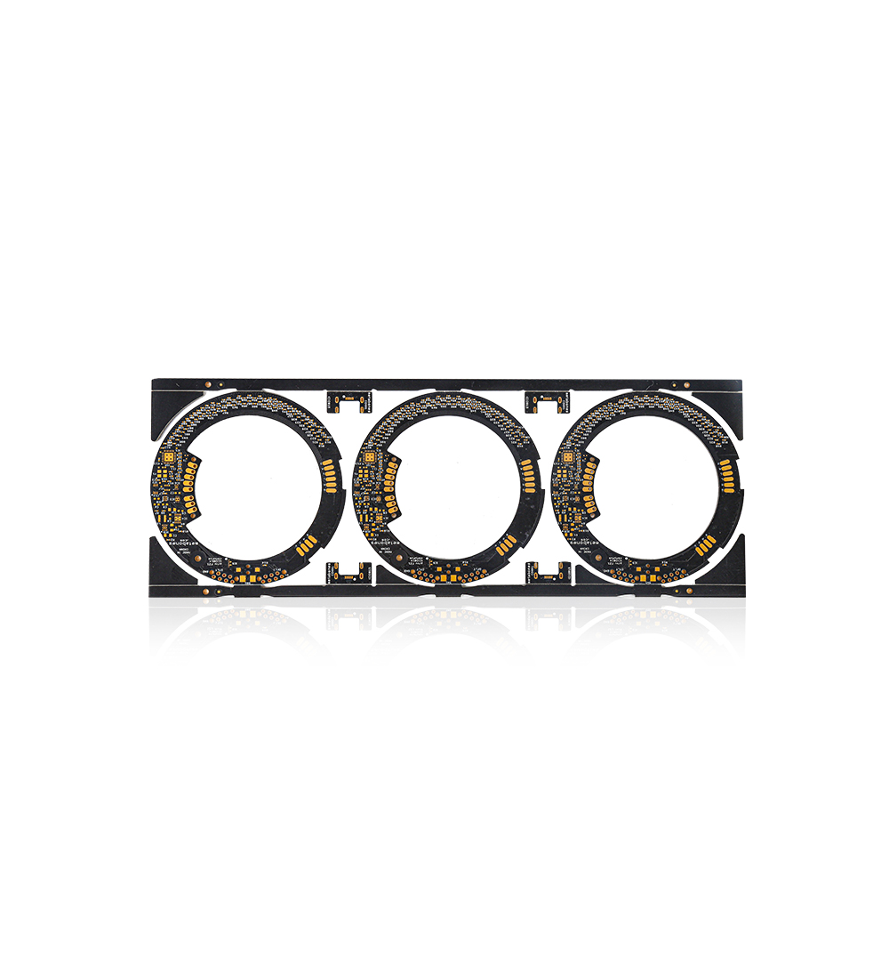
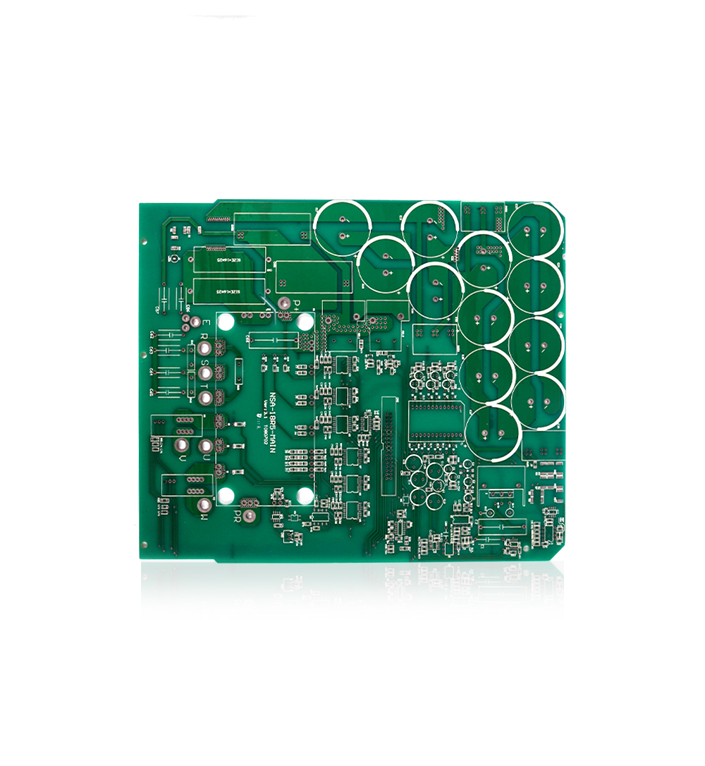
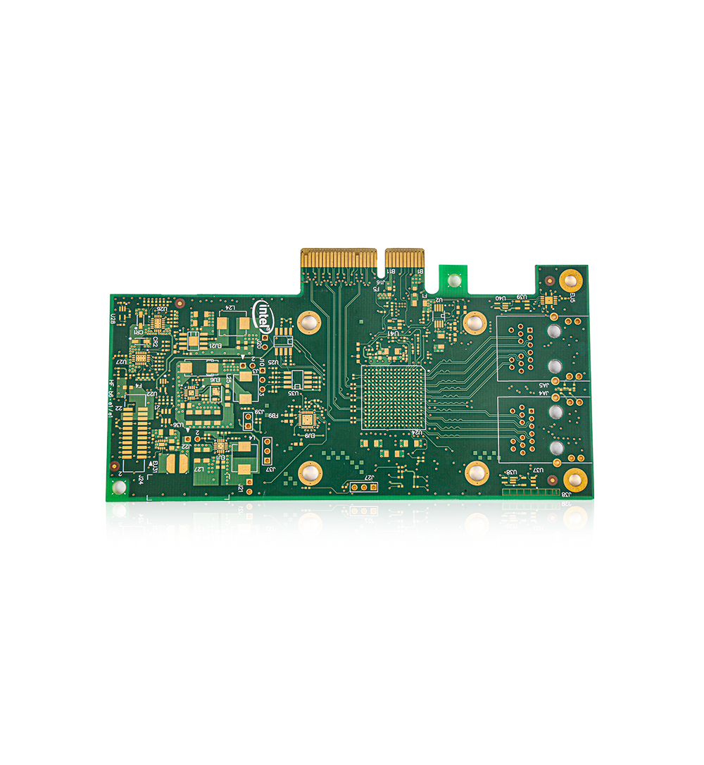
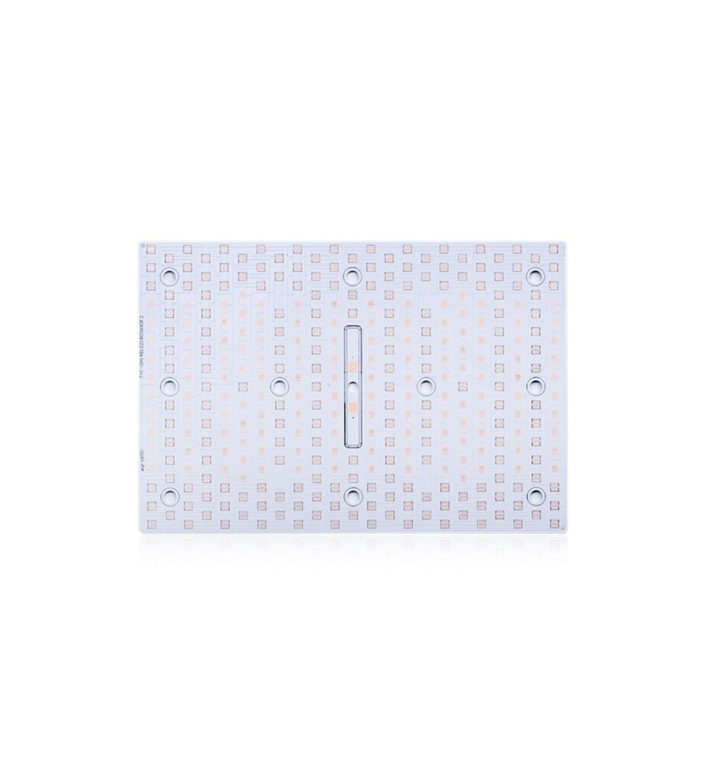
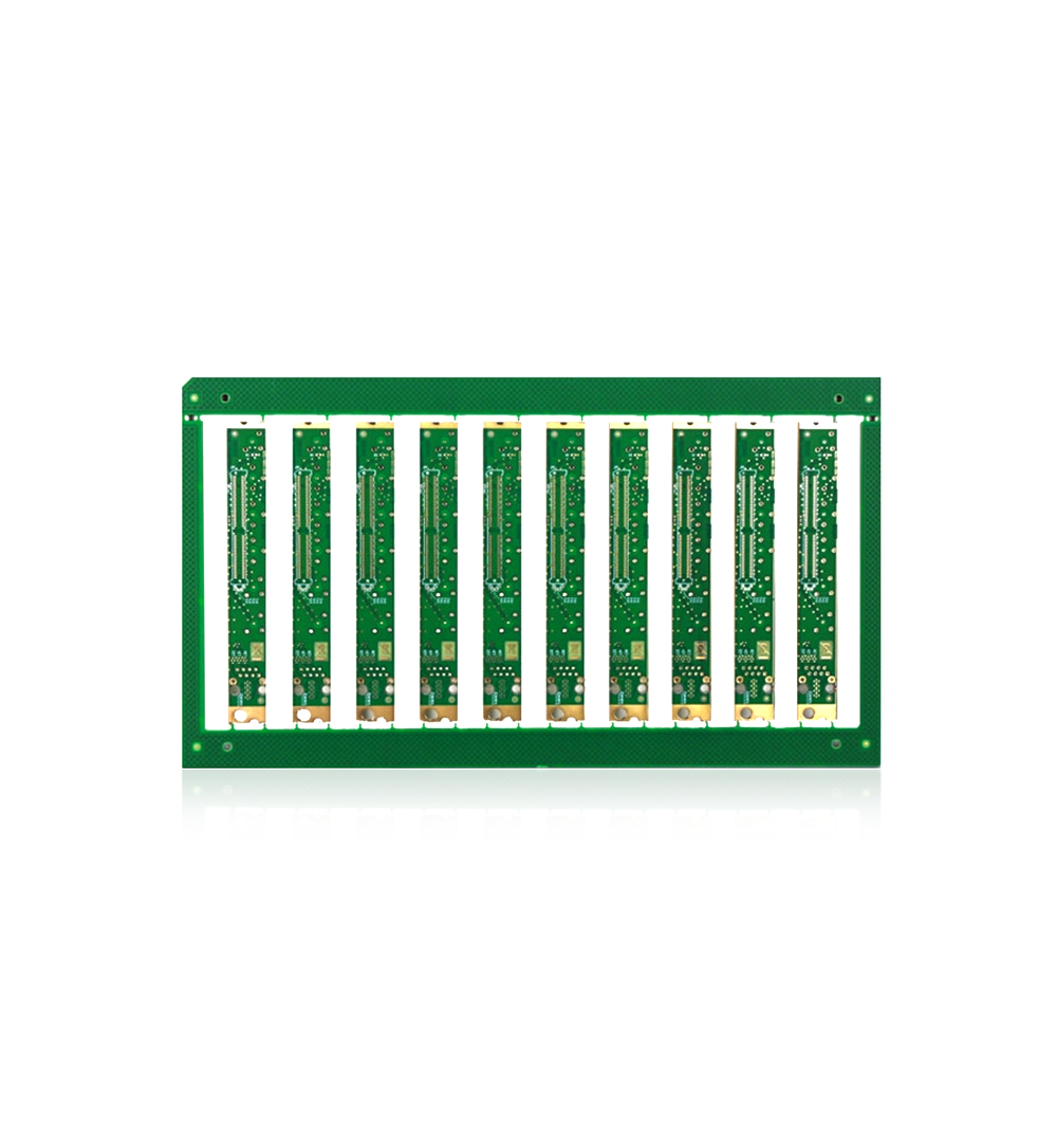
source:Other information release time:2022-11-11 Hits: Popular:PCB Assembly company

Step 1: Check data
Before production, the circuit board manufacturer will check the board making data provided by the customer, including the size of the board, process requirements, product quantity and other relevant data. The next step of production can only be carried out after reaching an agreement with the customer.
Step 2: Material opening
According to the plate making data provided by the customer, cut small pieces of production plates on the plates that meet the requirements. Specific operation: large plate → plate cutting according to MI requirements → curium plate → fillet/edge grinding → plate discharging.
Step 3: Drilling
Drill the required hole diameter at the corresponding position of the PCB. Large plate → cut plate according to MI requirements → curium plate → fillet/edge grinding → plate out.
Step 4: Copper sinking
A thin layer of copper is chemically deposited on the insulating hole. Specific operation: rough grinding → hanging plate → copper automatic line → lower plate → dipping 1% dilute H2SO4 → thickening copper.
Step 5: Graphic transfer
Transfer the image on the production film to the board. Specific operation: hemp board → film pressing → standing → alignment → exposure → standing → shadow developing → inspection.
Step 6: Pattern electroplating
Electroplate a copper layer with the required thickness and a gold nickel or tin layer with the required thickness on the exposed copper sheet or hole wall of the circuit diagram. Specific operation: upper plate → degreasing → secondary water washing → micro etching → water washing → pickling → copper plating → water washing → pickling → tin plating → water washing → lower plate.
Step 7: Film stripping
Remove the anti electroplating coating with NaOH solution to expose the non line copper layer.
Step 8: Etching
Remove the non line parts with chemical reagent copper.
Step 9: Green oil
The graphic of the green film is transferred to the board, mainly to protect the circuit and prevent the tin on the circuit when welding parts.
Step 10: Characters
Print recognizable characters on PCB. Specific operation: after green oil final curium → cooling and standing → screen adjustment → character printing → back curium.
Step 11: Gilded fingers
A nickel/gold layer of required thickness shall be plated on the plug finger to make it more hard and wear-resistant.
Step 12: Forming
The shape required by the customer is stamped with a die or produced by a numerical control gongs machine.
Read recommendations:
Welcome information, we will answer for you quickly

 No. 1 Jingtian Road, Xinsheng community, Longgang District, Shenzhen, Guangdong, China
 +86 13715096176
 Whatsapp/WeChat : +86 13715096176
 Kevin.kuang@xzgcircuits.com


 Return