source:Other information release time:2023-06-15 Hits: Popular:PCB Assembly company

You can understand the characteristics of selective welding by comparison with the peak welding. The most obvious difference between the two is that the lower part of the PCB in the peak welding is completely immersed in liquid solder, and in selective welding, only some specific areas are in contact with weld waves. Because PCB itself is a bad thermal conductivity, it does not heat the melt -melting neighboring component and PCB area welding joints during welding. Before welding, you must also apply the welding pre -welding. Compared with wave welding, the welded agent only coated at the lower part of the welding part of the lower part of the PCB, not the entire PCB. In addition, selective welding is only suitable for welding of inserted elements. Selective welding is a new method that thoroughly understands that selective welding processes and equipment are necessary for successful welding.
Selective welding process
Typical selective welding processes include: sprinkler spray, PCB preheat, soaked and mop welding.
Preheating process
Welding coating process
In selective welding, the coating process of the welded agent plays an important role. At the end of welding heating and welding, the welded agent should have sufficient activity to prevent bridges from generating and prevent PCB from oxidizing. The welding spray was carried by the X/Y robotic hand to carry the PCB above the top of the welded nozzle, and the welded agent was sprayed on the PCB to the welding position. The welds have a single -mouth spray type, microporous jet type, synchronous multi -point/graphic spray. The microwave peak selected welding after the return welding process is the most important thing is to accurately spray the welds. Micro -hole jet type will definitely not stain the area outside the welding joint. The diameter of the minimum welding point of the micro -point spray is greater than 2mm, so the location accuracy of the welding deployed on the PCB is ± 0.5mm to ensure that the solder is always covered on the welded area. The amount of welded doses is generally recommended for 100%safety tolerance range.
Read recommendations:
Halogen Free FR4 Multilayer Printed Circuit Board 1.6mm 10mil Impedance Control
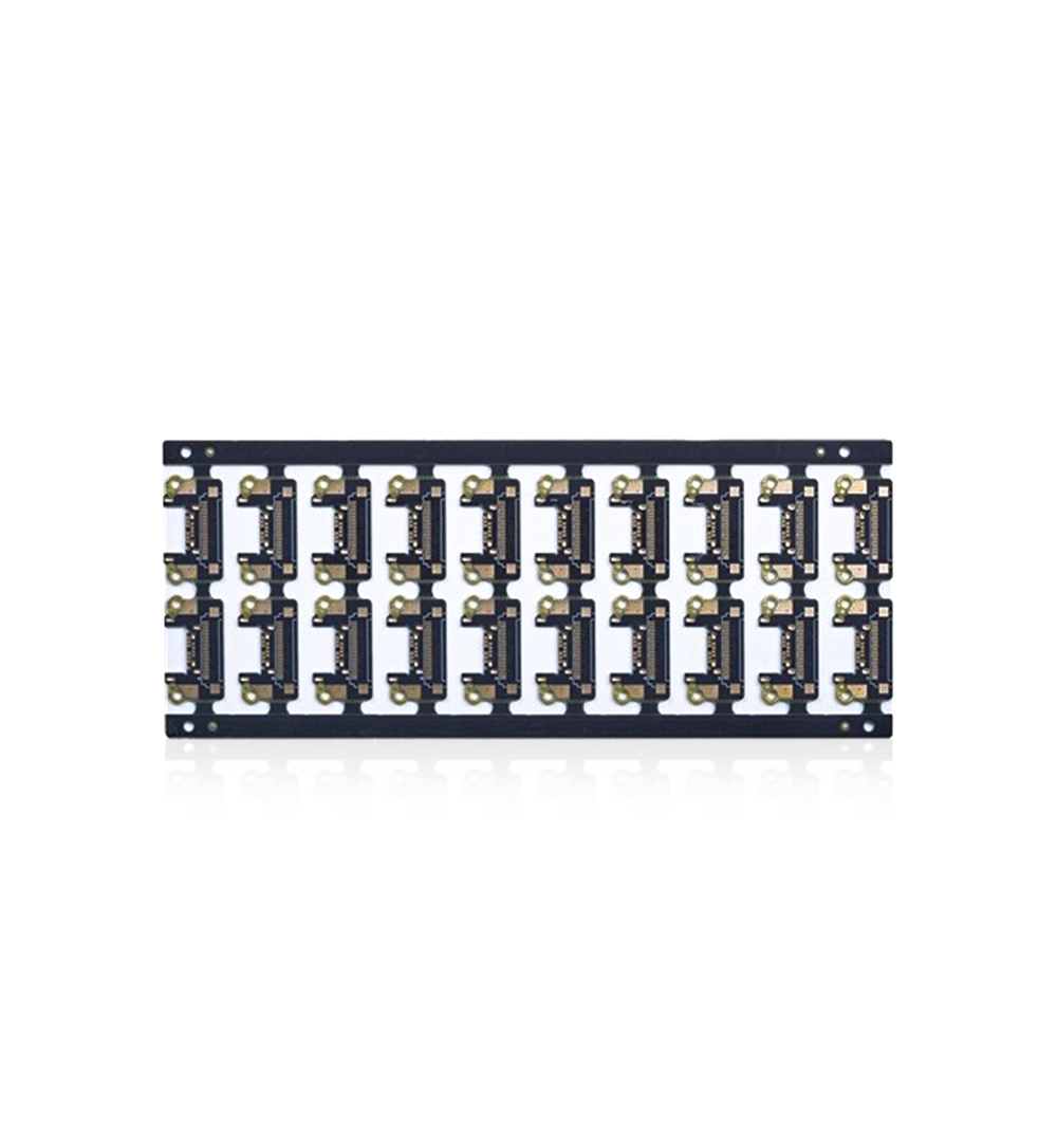
Polymer Film Flex PCB Board Double Sided 3mil 1oz ENIG Finished
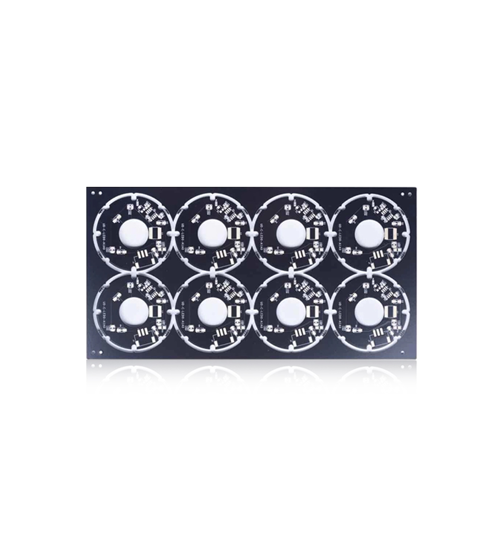
1.6mm OSP Aluminum Circuit Board Single Sided Pcb Board Lightweight
Welcome information, we will answer for you quickly

 No. 1 Jingtian Road, Xinsheng community, Longgang District, Shenzhen, Guangdong, China
 +86 13715096176
 Whatsapp/WeChat : +86 13715096176
 Kevin.kuang@xzgcircuits.com


 Return