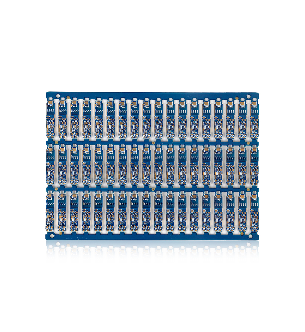
source:Other information release time:2023-05-10 Hits: Popular:PCB Assembly company

1) Pay attention to the hole on the board. Tongtong makes it necessary to etch on the opening on the power layer in order to leave the space you pass through the holes. If the power layer is too large, it will inevitably affect the signal circuit, forcing the signal bypass, the increase in the circuit area, and the increase in noise. At the same time, if some signal cables are concentrated near the opening and shared the circuit of the section, public impedance will cause string disturbances.
2) Place the power noise filter. It can effectively inhibit the internal noise of the power and improve the anti -interference and security of the system. In addition, it is a two -way radio frequency filter that can not only filter the noise interference introduced by the power cord (prevent interference of other equipment), but also remove the noise generated by itself (avoid interference with other devices), inhibit the serial mode Common model interference.
3) Power isolation transformer. The power loop or co -module of the separation signal cable can effectively isolate the co -mode circuit current generated by high frequency.
4) Power regulator. Re -obtaining cleaner power can greatly reduce power noise.
5) Wiring. The input and output cable of the power supply should not be arranged on the edge of the electronics board, otherwise it is easy to generate radiation and interfere with other circuits or equipment.
6) Simulation power and digital power supply should be separated. High -frequency devices are usually very sensitive to digital noise, so they should be separated and connected at the entrance of the power supply. If the signal spans analog and digital parts, the ring circuit can be set at the cross -section to reduce the ring area.
7) Avoid overlapping independent power supply between different layers. Try to staggered them, otherwise the power noise is easy to couple through parasitic capacitors.
8) Isolation sensitive element. Some components, such as locks, are very sensitive to power noise. They should stay away from the power as much as possible.
9) The connection line requires enough ground lines. Each signal requires its own special signal ring circuit. The area of the signal and ring circuit should be as small as possible, that is, the signal and the ring circuit should be parallel.
10) Place the power cord. In order to reduce the signal loop, the noise can be reduced by closer the power line near the signal line.
Device.
Read recommendations:
Polymer Film Flex PCB Board 0.1mm 2 Layer Rigid Flex Pcb Lightweight
Welcome information, we will answer for you quickly

 No. 1 Jingtian Road, Xinsheng community, Longgang District, Shenzhen, Guangdong, China
 +86 13715096176
 Whatsapp/WeChat : +86 13715096176
 Kevin.kuang@xzgcircuits.com


 Return