source:Other information release time:2022-12-01 Hits: Popular:PCB Assembly company

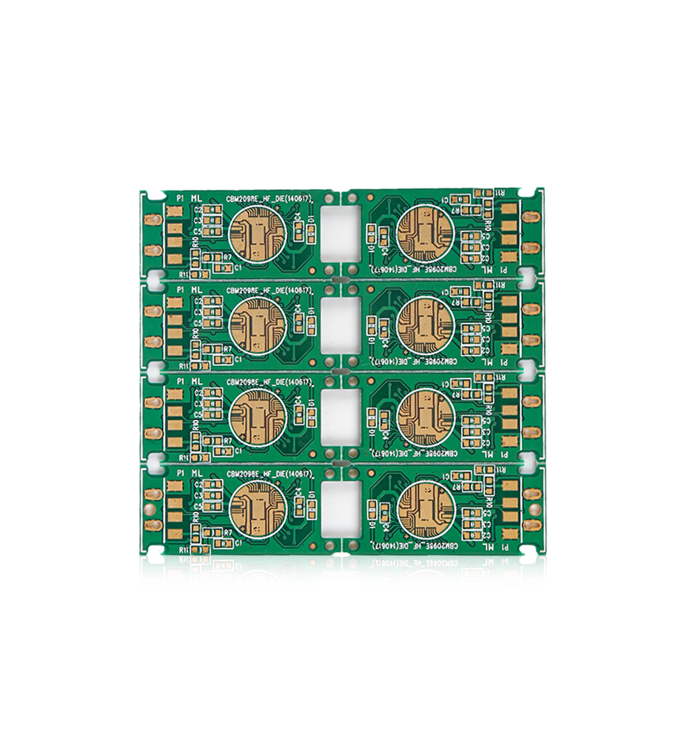
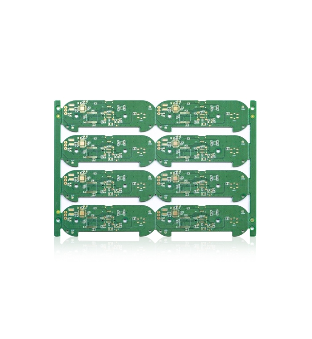
In terms of fields, many Shenzhen PCB factories only do one or two application fields, while some can do PCB in multiple application fields. Circuit board manufacturers (Shenzhen Zhongke Circuit) can produce high-precision multilayer circuit boards in high-tech applications such as industrial control, communication, medical, military, security, aerospace, etc. From the structure of the circuit board, it can also be made into single and double sided circuit boards and PCB multilayer circuit boards. Today, Shenzhen PCB Factory focuses on introducing the application field and structure of multilayer PCB.
1. Section Geometry of Multilayer PCB
Multilayer printed circuit boards can have single side, double side, four layer, six layer, eight layer structures according to the number of layers of the circuit. As for the recently mentioned high-density HDI circuit board, because the usual production method is to build a core hard board in the center, and on this basis, grow layers up and down on both sides. Therefore, there are two common names. One is to use the number of hard board layers in the center as the first number, and the number of wire layers added on both sides as the other number. Therefore, there are so-called descriptions of 4+2, 2+2, 6+4, etc. However, another name may make it easier for people to understand the actual situation. Because most multi-layer circuit board designs explore symmetric design, we will explore the names of 1+4+1, 3+6+3, etc. At this time, if someone says that a 2+4 structure may be an asymmetric structure, we must confirm it.
2. Connection mode between multilayer circuit boards
The circuit board establishes the metal layer in an independent circuit layer, so the longitudinal connection between layers is indispensable. In order to achieve the purpose of interlayer connection, it is necessary to use drilling method to form a path and form a reliable conductor on the hole wall to complete the connection of power or signals. Since through-hole electroplating was proposed, almost all multilayer circuit boards have been produced by this method.
The increased density multilayer circuit board is fabricated by using the layer adding mode. The method is to form small holes on the dielectric material by laser or photosensitive method, and then conduct it by electroplating. Some manufacturers fill the connecting holes with conductive adhesive to achieve continuity, such as ALIVH and B2it developed in Japan.
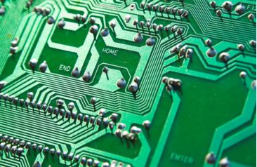
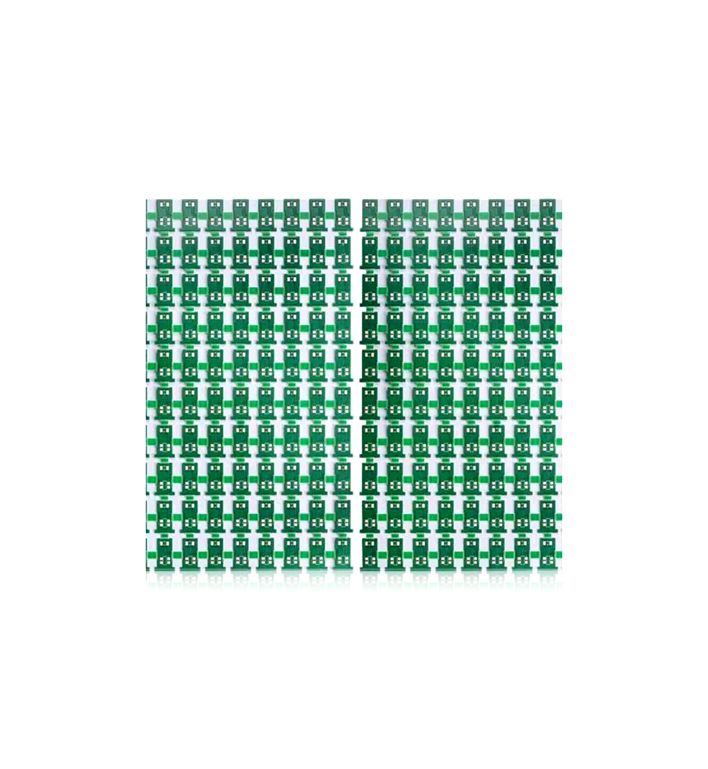
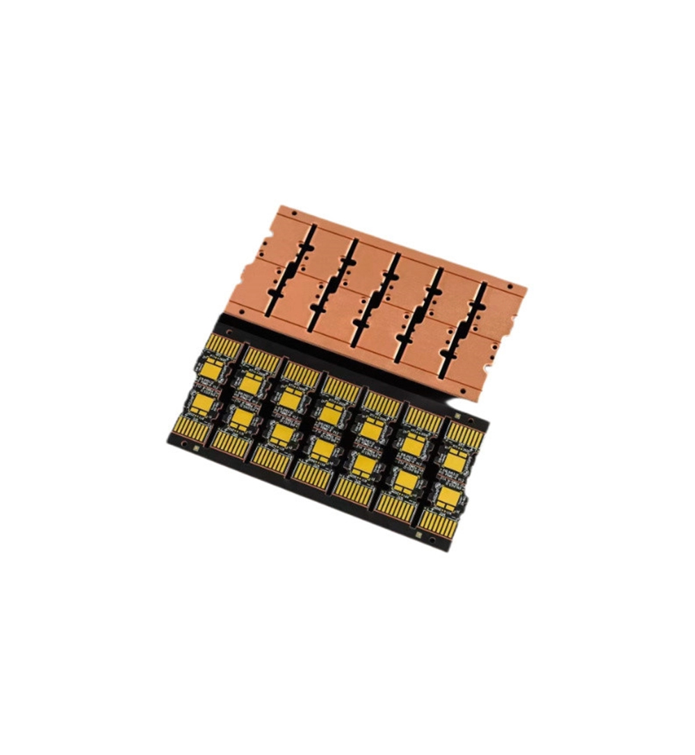
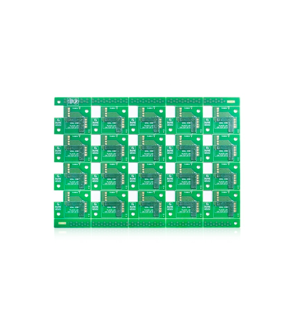
3. Application field of multilayer circuit board
PCB multilayer printed circuit boards generally focus on electroplating through holes. The number of layers, thickness, and hole location configuration of PCB multilayer printed circuit boards vary with the circuit density. The classification of their specifications and contents is based on this. The soft and hard combination plates are mostly used in military, aerospace and instrument equipment. Under the premise that electronic products tend to be multi-functional and complex, the contact distance of integrated circuit components will be reduced, and the speed of signal transmission will be relatively improved, followed by an increase in the number of wiring and a local reduction in the length of wiring between points. These require high-density circuit configuration and microporous technology to achieve the goal. Wiring and jumper are basically difficult to achieve for single and double sided circuit boards, so the circuit boards will move towards multi-layer; Because of the increasing number of signal lines, more power supply layers and ground layers have become the necessary means of design, which has made multilayer printed circuit boards more common.
Pcb multilayer circuit board factory: a method to strengthen anti-interference capability
To achieve the best performance of electronic circuits, electronic component circuit boards are the supporting parts of circuit components and devices in electronic products. Even if the circuit schematic is correctly designed and the printed circuit board is improperly designed, the reliability of electronic products will be adversely affected. When designing printed circuit boards, it is important to adopt correct methods, follow the general principles of PCB design, and meet the requirements of anti-interference design. In order to design PCB boards with good quality and low cost, the following general principles should be followed:
First, the size of pcb multilayer circuit board should be considered. When the size of pcb multilayer circuit board is too large, the printed line is long, the impedance increases, the anti noise ability decreases, and the cost increases; If it is too small, the heat dissipation is poor, and adjacent lines are vulnerable to interference. After determining the size of pcb multilayer circuit board, determine the location of special components. Finally, all components of the circuit are arranged according to the functional unit of the circuit.
Read recommendations:
Polymer Film Flex PCB Board Double Sided 3mil 1oz ENIG Finished
Immersion Gold IPC Class 3 PCB Double Sided Green Solder Mask 4mil 1.6mm
Welcome information, we will answer for you quickly

 No. 1 Jingtian Road, Xinsheng community, Longgang District, Shenzhen, Guangdong, China
 +86 13715096176
 Whatsapp/WeChat : +86 13715096176
 Kevin.kuang@xzgcircuits.com


 Return