source:Other information release time:2023-02-06 Hits: Popular:PCB Assembly company

With the requirements of electronic products for volume, especially the size of the mobile device products in the direction of continuously shrinking, such as the current popular Ultra Book products, and even novel wearable smart devices, must use the HDI line board height height The carrier board produced by density interconnection technology further lowered the product size.
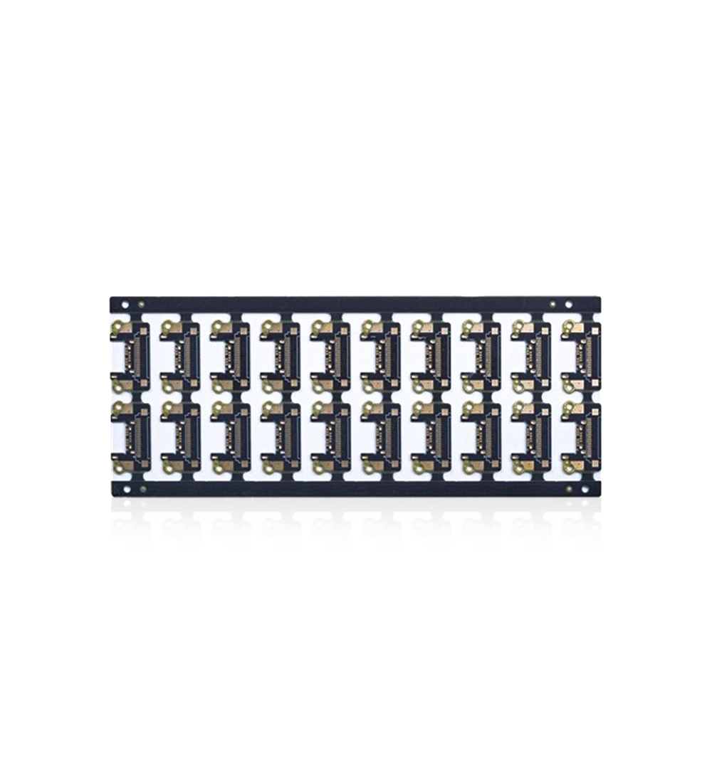
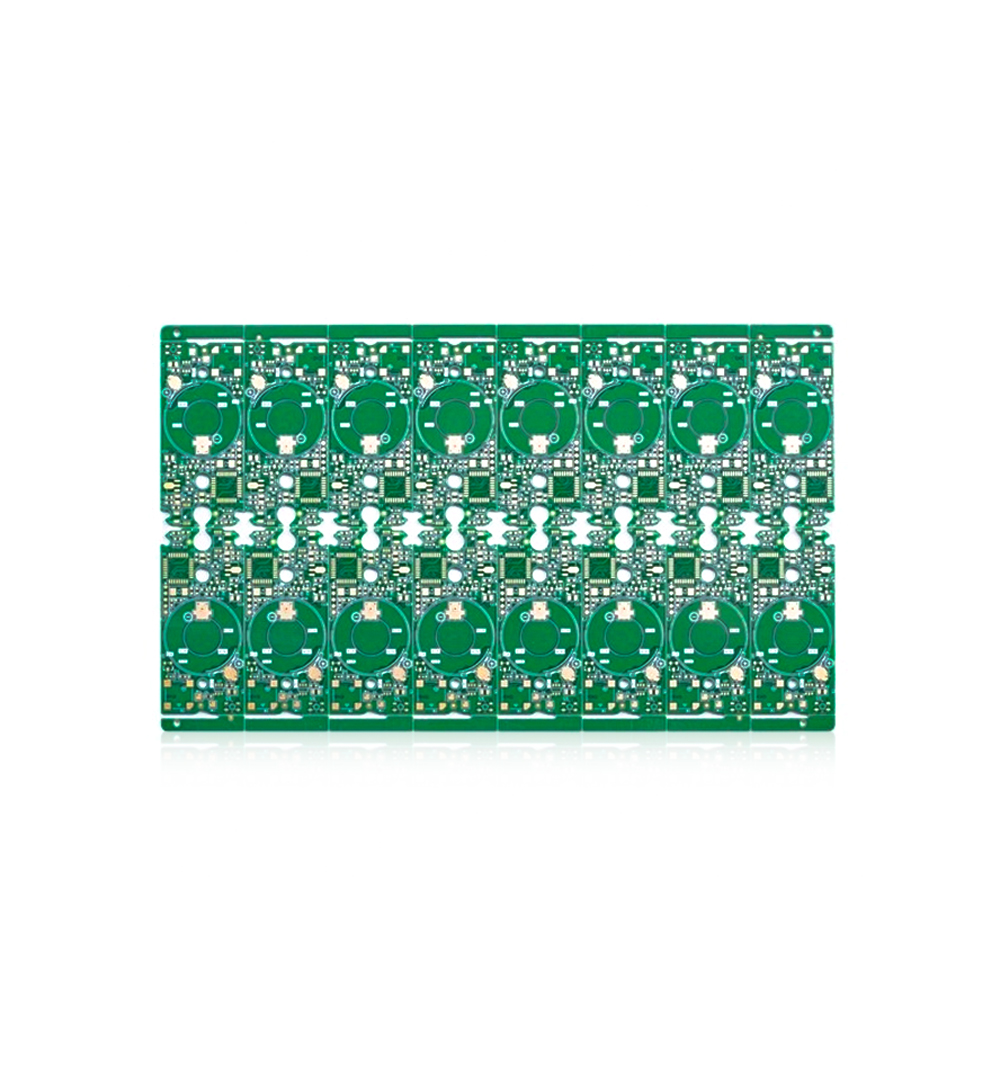
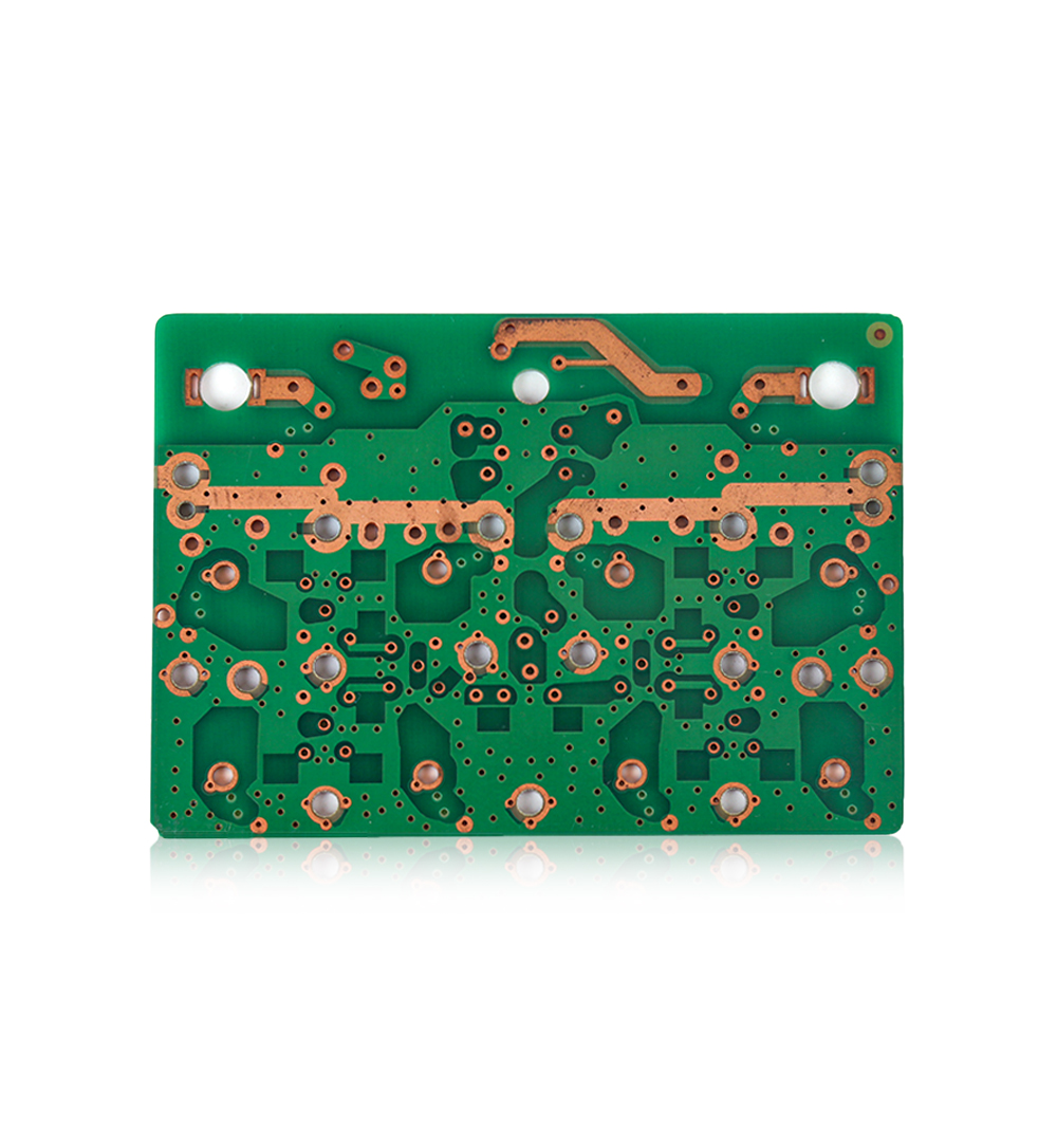
The HDI circuit board is a high -density interconnection technology, which is one of the technology used by printing circuit boards. HDI is mainly used to make the technology of micro -blind holes. The characteristic is that the density of the electronic circuit distribution line in the printing circuit board is higher. Due to the large increase in the density of the line, the printing circuit board made of HDI cannot be used in general drilling The hole method is perforated. HDI must adopt non -mechanical drilling processes. There are quite many methods for non -mechanical drilling. Among them, "laser" is the main combination of HDI high -density interconnection technology.
The application field of HDI printing circuit boards is quite wide. For example, electronic products such as mobile phones, ultra -thin laptops, tablets, digital cameras, vehicle electronics, digital cameras, etc. have all used HDI technology to narrow the motherboard design, reduced the benefits of the benefits Quite large, not only the design of the terminal product can leave more space in the institution to batteries, or more additional functional components, the cost of the product can also be relatively reduced due to the import of HDI.
Read recommendations:
Green Solder Mask FR4 Single Sided PCB Board 0.4mm Halogen Free
Welcome information, we will answer for you quickly

 No. 1 Jingtian Road, Xinsheng community, Longgang District, Shenzhen, Guangdong, China
 +86 13715096176
 Whatsapp/WeChat : +86 13715096176
 Kevin.kuang@xzgcircuits.com


 Return