source:News release time:2023-05-09 Hits: Popular:PCB Assembly company

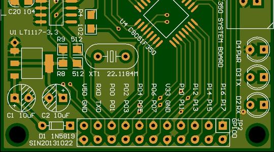
(1) The size of the pad
The size of the pad is related to factors such as the lead hole and the width of the minimum hole. The size of the pads should be increased as much as possible, but the wiring density should be considered at the same time. In order to ensure the reliability of the pad and the substrate connection, the pore drill is in the center of the pads, and the pore diameter should be slightly larger than the diameter of the welding element lead. The diameter of the device's leading hole is preferentially adopted by 0.5 mm, 0.8 mA △ and 1.2 mm. The width of the pad ring is selected in the range of 0.5 to 1.0 mm. Generally, the diameter size of the pads of the dual -column direct -integrated circuit is 1.5 to 1.6 mm, and the printed wires that can be passed by 0.3 to 0.4 mm can be passed between adjacent pads. The ring width of the general pads is not less than 0.3 mm, and the diameter of the pads is not less than 1.3 mm. The actual pads are selected for the parameters recommended by Table 8-1.
(2) The shape of the pad
Select different shapes of pads according to different requirements. Common pads are round, square, ellipse, island and alien, etc., as shown in Figure 10.
Round pad: The outer diameter is generally 2 to 3 times the aperture, and the pore diameter is greater than 0.2 to 0.3 mm.
Island pad: The connection between the pad and the pads is integrated, like a small island, so it is called an island pad. It is often used in irregular arrangements for components, which is conducive to densely fixing components, and can reduce the length and quantity of the printed wires in large quantities. Therefore, it is mostly used in high -frequency circuits.
Other forms of pads are made to make the printed wires passing through the adjacent pads, and the circular pads are deformation. Use it flexibly according to the actual situation.
Read recommendations:
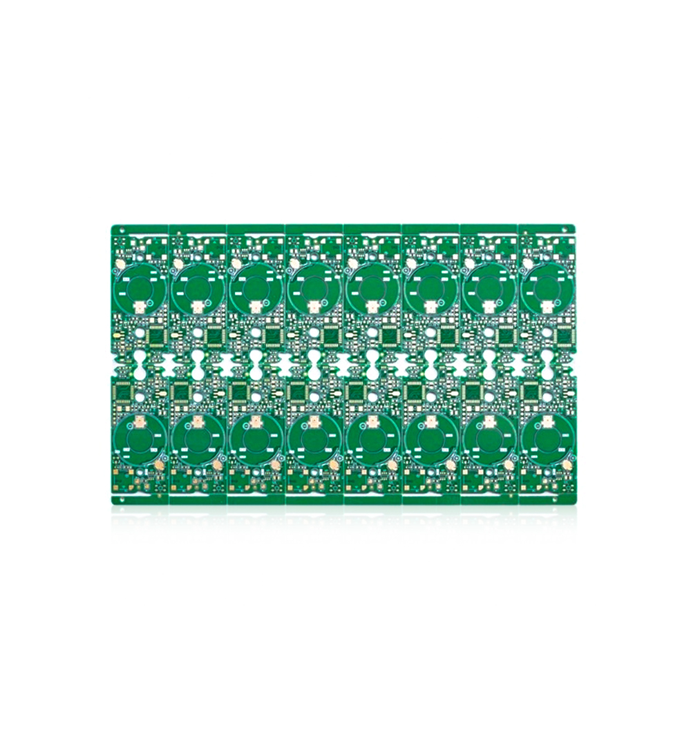
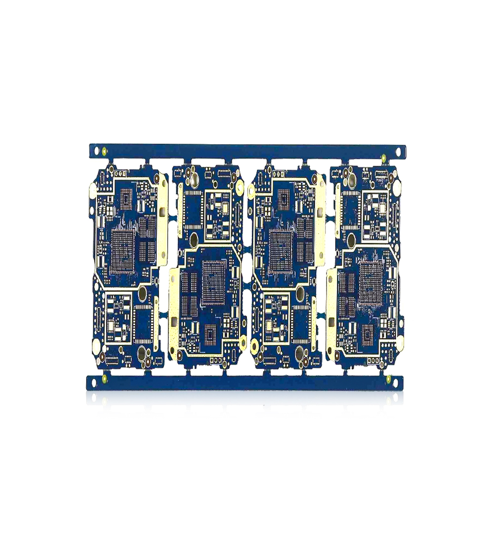
Multilayer Printed Circuit Board 1OZ 4 Layer Multilayer Pcb FR4 TG170 Blue Solder Mask
Lightweight Aluminum PCB Board Green Solder Mask Led Light Pcb Board 3.0mm
HASL FR4 Single Sided Copper PCB Board White Solder Mask 35um Thickness
Welcome information, we will answer for you quickly

 No. 1 Jingtian Road, Xinsheng community, Longgang District, Shenzhen, Guangdong, China
 +86 13715096176
 Whatsapp/WeChat : +86 13715096176
 Kevin.kuang@xzgcircuits.com


 Return