source:Other information release time:2023-04-23 Hits: Popular:PCB Assembly company

The over -holes in high -speed PCB are analyzed by the above -mentioned perforated parasitic characteristics. We can see that in high -speed PCB design, seemingly simple holes often bring a great negative effect to the design of the circuit. In order to reduce the adverse effects of the parasitic effect of the holes, you can do it as much as possible in the design:
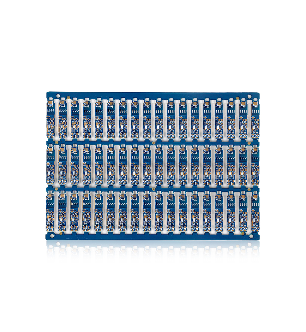
1. Considering the two aspects of cost and signal quality, select the excessive hole size of the reasonable size. For example, for the PCB design of the 6-10-layer memory module, the use of 10/20mil (drilling/pad) is better. For some high-density small-sized boards, you can also try to use the excess of 8/18mil hole. Under the current technical conditions, it is difficult to use smaller -sized perforated. For the over -holes of the power supply or ground line, you can consider using larger sizes to reduce impedance.
2. The two formula discussed above can be concluded that using a thin PCB board is conducive to the two parasitic parameters that reduce holes.
3. Try not to change the signal wiring on the PCB board, that is, try not to use unnecessary perforated.
4. The pipes of the power supply and the ground should be played nearby. The shorter the lead between the perforated and the tube, the better, because they will increase the inductance. At the same time, the lead of the power and land should be as thick as possible to reduce impedance.
5. Place some ground -to -holes near the extension of the signal change to provide nearby circuits for the signal. You can even place some excess ground holes on the PCB board. Of course, it is necessary to be flexible when designing. The pellet model discussed earlier is that there are pads in each layer, and sometimes we can reduce or even remove the pads of some layers. Especially in the case of high -perforated density, it may lead to forming a disconnection of a partition circuit in the copper layer. In addition to the position of such problems, we can also consider putting the holes on the copper layer of the paved layer. The size of the pad is reduced.
Read recommendations:
1.6mm HASL OSP Multi Layer Pcb Board FR4 Halogen Free Green Solder Mask
Immersion Gold IPC Class 3 PCB Double Sided Green Solder Mask 4mil 1.6mm
Welcome information, we will answer for you quickly

 No. 1 Jingtian Road, Xinsheng community, Longgang District, Shenzhen, Guangdong, China
 +86 13715096176
 Whatsapp/WeChat : +86 13715096176
 Kevin.kuang@xzgcircuits.com


 Return