source:Other information release time:2023-02-03 Hits: Popular:PCB Assembly company

1. Layer pressure is the process of bonding the lines of each layer into the overall layer with the help of B-order semi-solidifying tablets. This bonding is achieved through the mutual spread and penetration between the macromolecules on the interface, and then generates interwovenness. The order semi -cured tablets bond the lines of each layer into the overall process. This bonding is the mutual diffusion and penetration between the macromolecularly spreading between the large molecules on the interface, and then produce mutual interweaving.
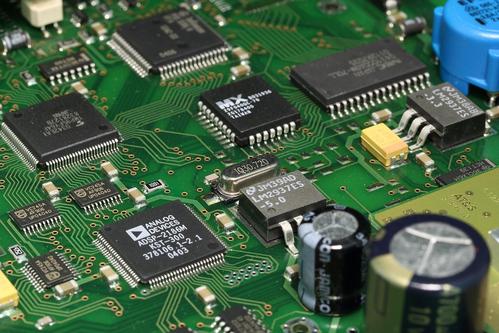
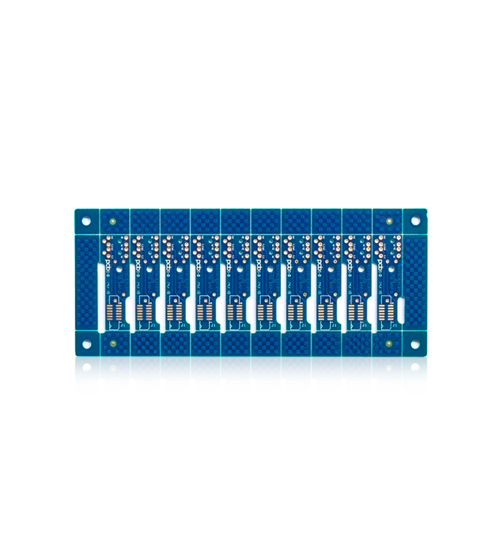
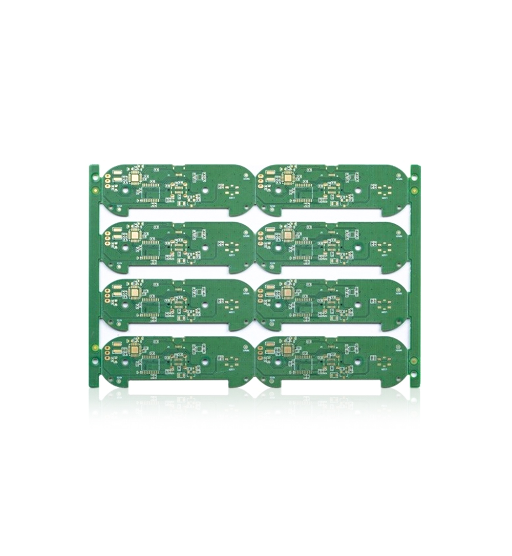
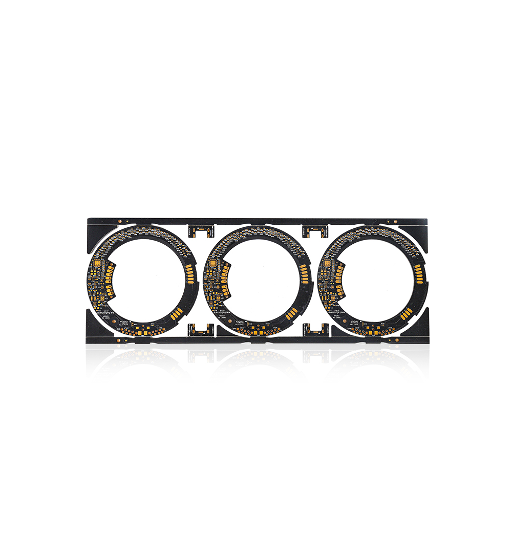
2. Purpose: Press the discrete multi -layer PCB board with the sticky chip into a multi -layer board required for the number of layers and thickness.
① Send the stacked circuit board into the vacuum heat compressor process. Use the thermal energy provided by the machine to melt the resin in the resin tablet to bond the substrate and fill the gap.
② The typesetting of copper foil, adhesion (semi -curing tablets), inner plate, stainless steel, isolation plate, leather paper, outer steel plate and other materials are superimposed according to process requirements. If the board on the sixth layer line board is also needed to be pre -arranged.
③ For designers, layer pressure first needs to consider symmetry. Because the board will be affected by pressure and temperature during the layer pressure, there will be stress in the board after the layer pressure is completed. Therefore, if the two sides of the layer pressure are uneven, the stress on the two sides is different, causing the board to bend one side, which greatly affects the performance of PCB.
In addition, even in the same plane, if the distribution of copper is uneven, the resin flow of each point will be different, so that the thickness of the place with less copper will be slightly thinner, and the thickness of the places with more copper will be slightly thicker. Some. In order to avoid these problems, the factors of the uniformity of cloth copper, the symmetry of the overlapping layer, the design layout of the blind buried holes, and other aspects of the design must be detailed.
Read recommendations:
FR4 1.6mm Double Sided Prototype PCB Board Immersion Gold 4mil
Welcome information, we will answer for you quickly

 No. 1 Jingtian Road, Xinsheng community, Longgang District, Shenzhen, Guangdong, China
 +86 13715096176
 Whatsapp/WeChat : +86 13715096176
 Kevin.kuang@xzgcircuits.com


 Return