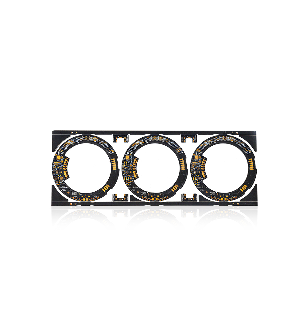
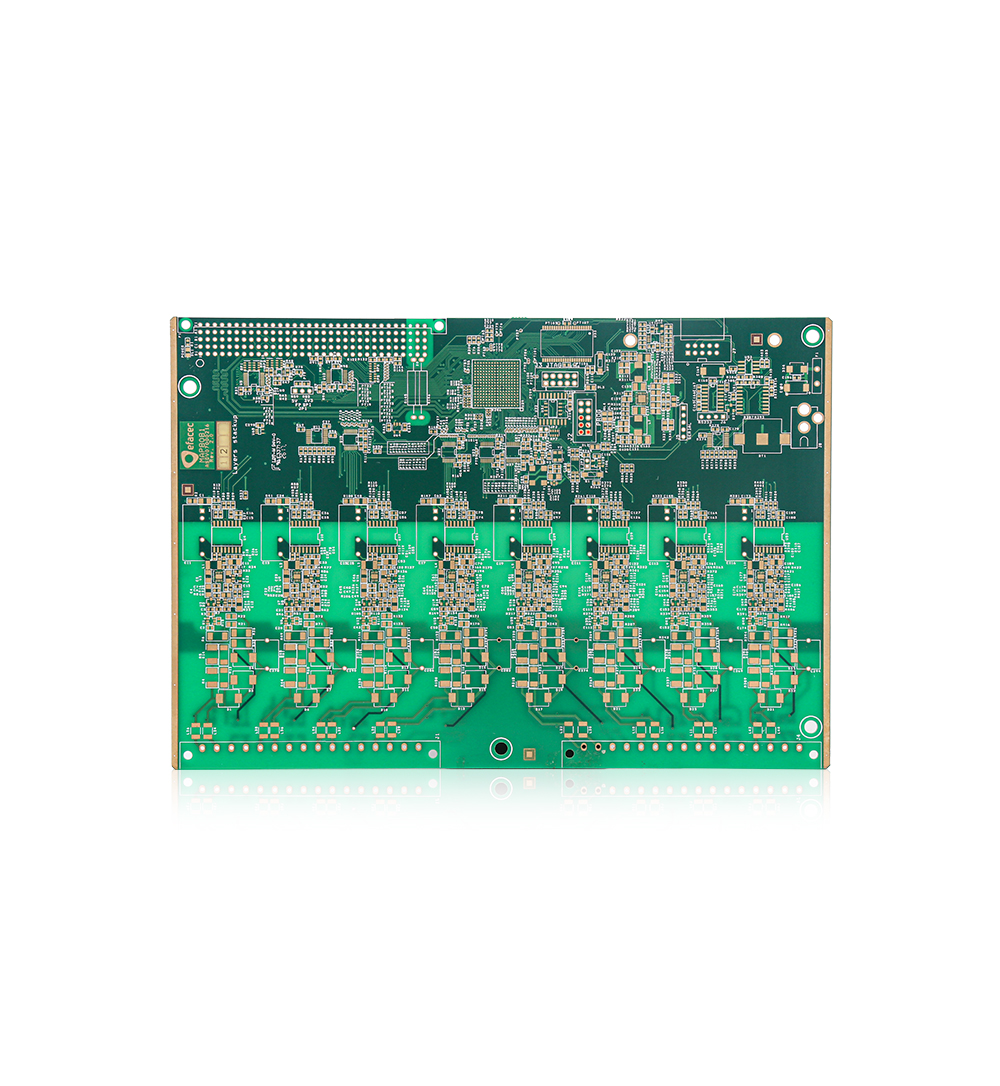
source:Other information release time:2023-05-24 Hits: Popular:PCB Assembly company

When you contact the 4 -layer PCB manufacturer, they will provide you with these two standard structures of the 4 -layer PCB. The VCC and GND layers here are organized according to the application requirements.
Type 1: Signal -GND -VCC -Signal: In this 4 -layer PCB design, the top layer is the best signal. In terms of layer thickness, the core board of impedance control should not be too thick. This helps reduce the distribution impedance of ground layers and power.
Type 2: GND -Signal -Signal -GND: If you don't want to connect all types of ground pins with a passing path, this stack structure is very ideal. In order to improve the EMC performance of the circuit board, it is a good idea to put the signal layer near the plane. Use the large core wire between the ground floor and the power layer to maintain the overall thickness of the substrate.
Read recommendations:
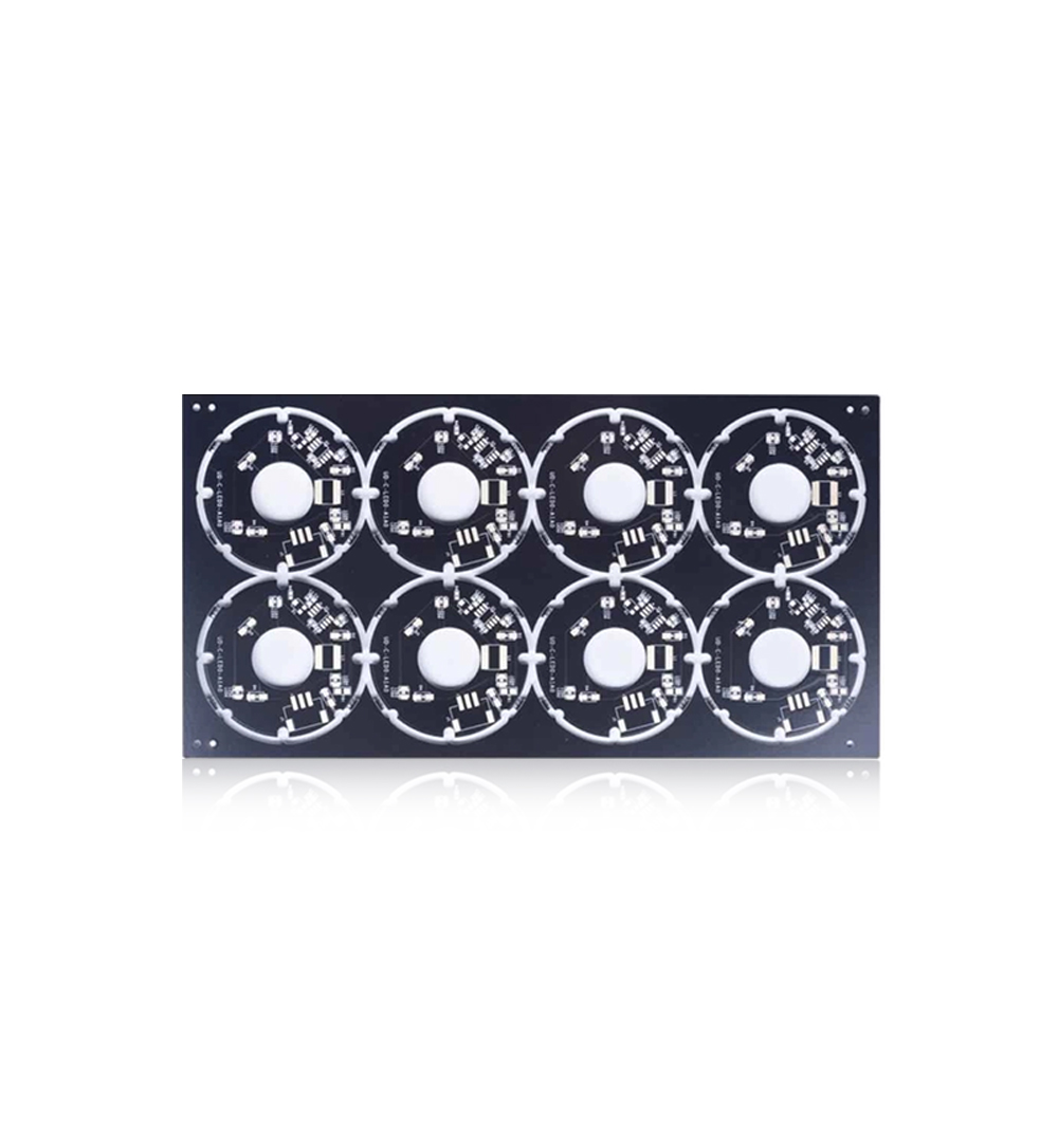
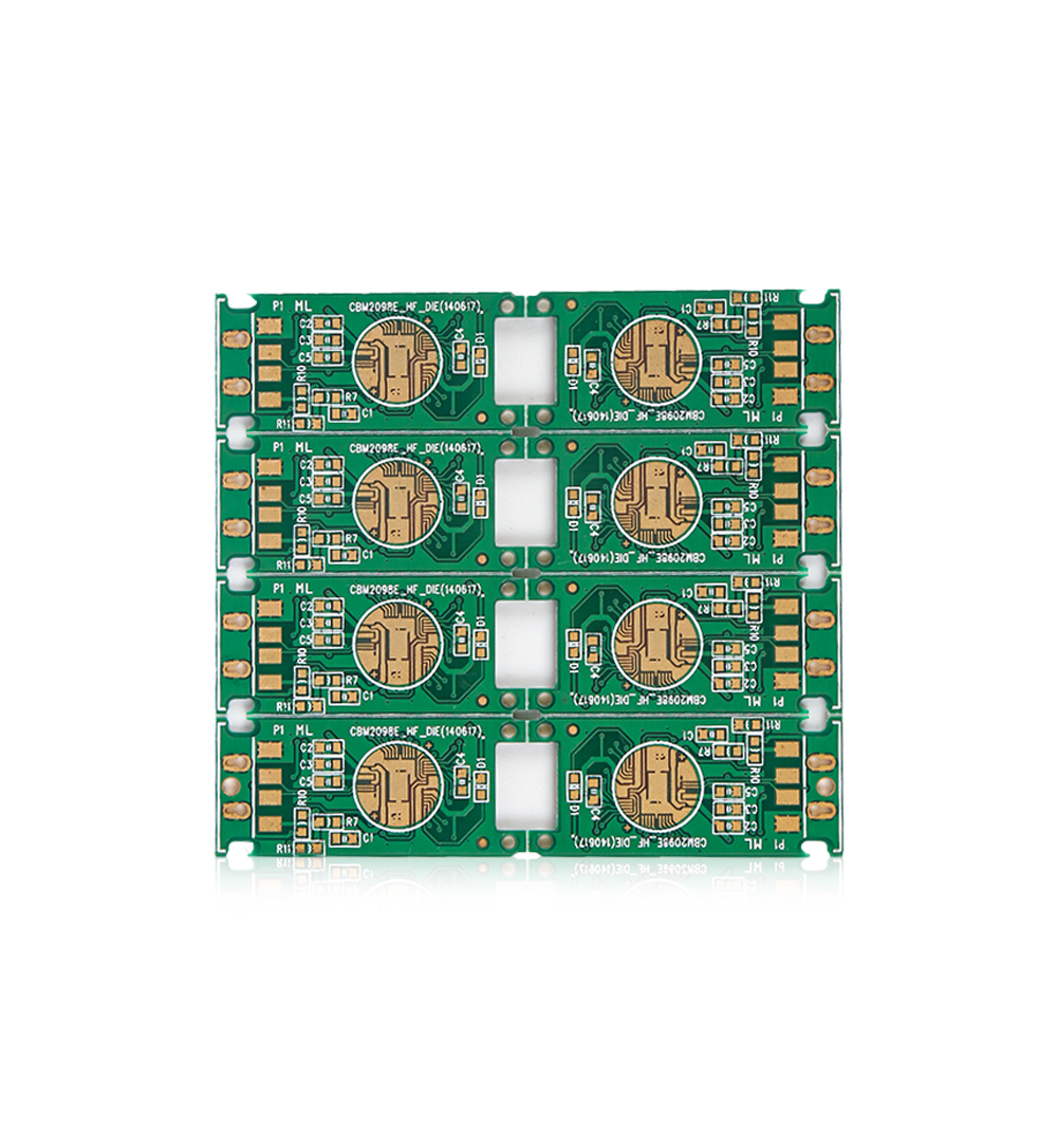
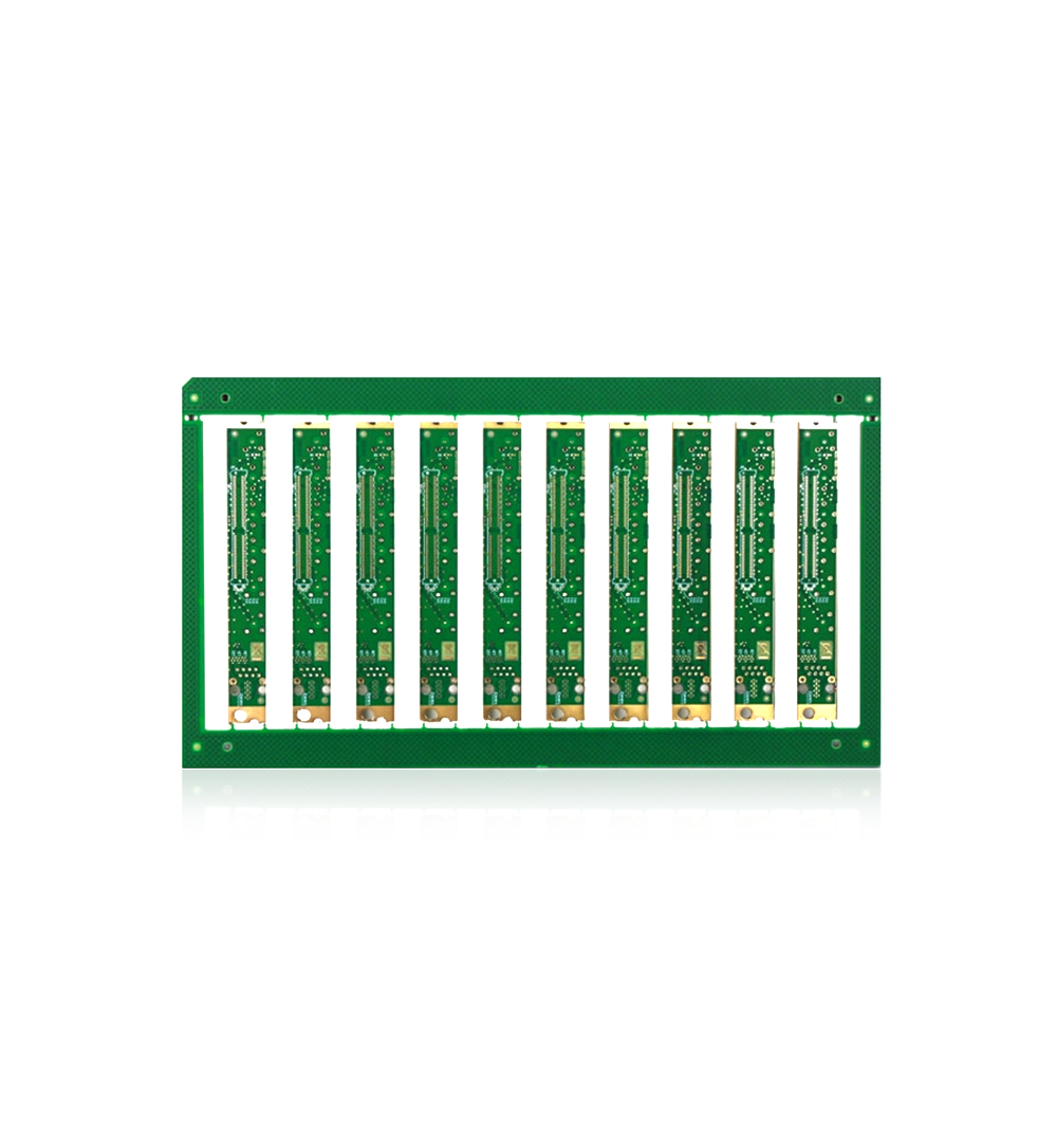
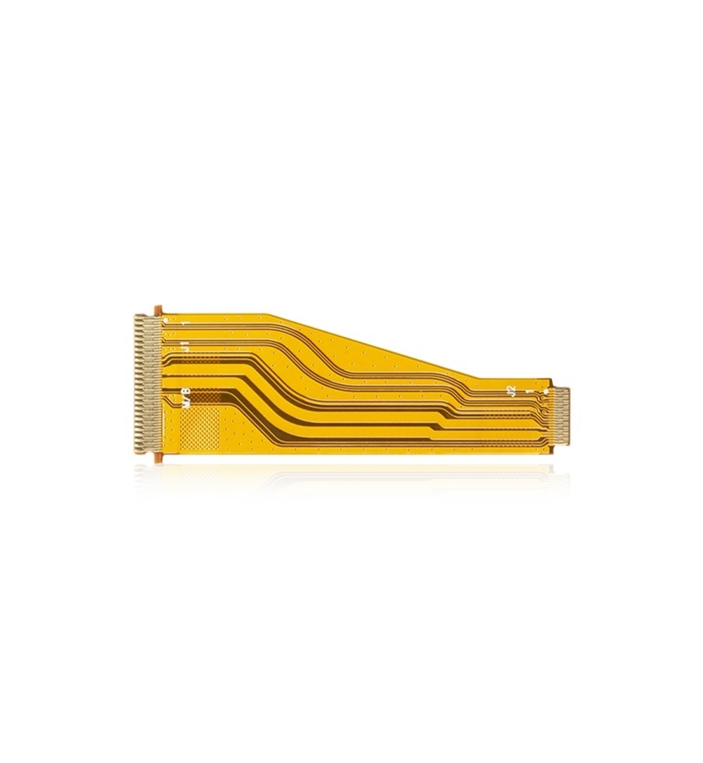
PI FR4 Double Layer Flex PCB Board Immersion Gold 2L Lightweight
Welcome information, we will answer for you quickly

 No. 1 Jingtian Road, Xinsheng community, Longgang District, Shenzhen, Guangdong, China
 +86 13715096176
 Whatsapp/WeChat : +86 13715096176
 Kevin.kuang@xzgcircuits.com


 Return