source:Other information release time:2023-02-02 Hits: Popular:PCB Assembly company

1、 Contact the manufacturer
First, you need to find the PCB manufacturer on the Internet, and then find out the company size, product advantages, and address of the PCB manufacturer. Then you can communicate (QQ or call), and there will be relevant personnel to quote for you, place an order, and follow up the production progress, shipment, and delivery.
2、 Material opening
Purpose: According to the requirements of the engineering data MI, cut the large plates that meet the requirements into small pieces for production. Small plates that meet customer requirements
Process: large plate → plate cutting according to MI requirements → curium plate → beer fillet edge grinding → plate out
3、 Drilling
Purpose: According to the engineering data, drill the required hole diameter at the corresponding position on the sheet metal with the required size
Process: laminated pin → upper plate → drilling → lower plate → inspection/repair
4、 Copperplate
Purpose: Copper deposition is to deposit a thin layer of copper on the wall of insulating hole by chemical method
Process: rough grinding → hanging plate → automatic copper deposition line → lower plate → dipping% dilute H2SO4 → thickening copper
5、 Graphic transfer
Purpose: Graphic transfer is to transfer the image on the production film to the board
Process: (blue oil process): plate grinding → printing the first side → drying → printing the second side → drying → lighting → developing → inspection; (Dry film process): hemp board → pressing film → standing → alignment → exposure → standing → developing → inspection
6、 Graphic electroplating
Purpose: Pattern electroplating refers to electroplating a copper layer with the required thickness and a gold nickel or tin layer with the required thickness on the exposed copper skin or hole wall of the circuit pattern
Process: upper plate → degreasing → secondary water washing → micro etching → water washing → pickling → copper plating → water washing → pickling → tin plating → water washing → lower plate
7、 Demembrane
Purpose: Remove the anti electroplating coating with NaOH solution to expose the non circuit copper layer
Process: water film: rack inserting → alkali dipping → flushing → scrubbing → machine passing; Dry film: plate placing → machine passing
Read recommendations:
1OZ 1.0mm Aluminum PCB Board OSP Finished Aluminium Substrate Pcb
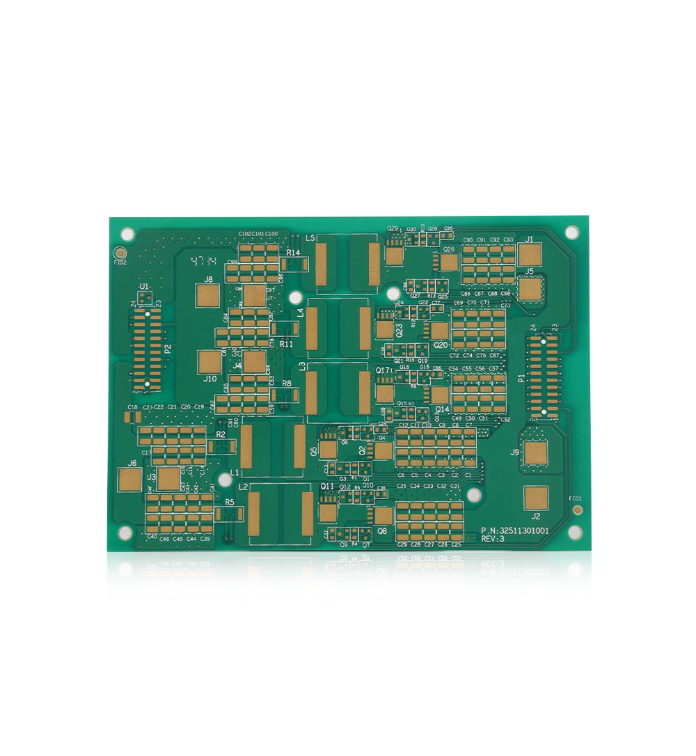
Multilayer Printed Circuit Board
Environmentally Friendly Aluminum PCB Board 1.6mm Single Layer
Welcome information, we will answer for you quickly

 No. 1 Jingtian Road, Xinsheng community, Longgang District, Shenzhen, Guangdong, China
 +86 13715096176
 Whatsapp/WeChat : +86 13715096176
 Kevin.kuang@xzgcircuits.com


 Return