source:News release time:2022-12-01 Hits: Popular:PCB Assembly company

The double-sided circuit board is a medium layer in the middle, and both sides are wiring layers. Pcb multilayer circuit board is a multilayer routing layer, between each two layers is a dielectric layer, and the dielectric layer can be very thin. The multilayer circuit board has at least three conductive layers, two of which are on the outer surface, and the remaining layer is synthesized in the insulating board. The electrical connection between them is usually realized through the plated through-hole on the cross section of the circuit board.
High assembly density, small size and light weight Because of high assembly density, the connection between components (including components) is reduced, so the reliability is improved; The number of cabling layers can be increased, thus increasing the design flexibility; Can form a circuit with a certain impedance; High speed transmission circuit can be formed; The circuit and magnetic circuit shielding layer can be set, and the metal core heat dissipation layer can also be set to meet the needs of special functions such as shielding and heat dissipation; Simple installation and high reliability.
High cost; Long cycle; High reliability detection means are required. Multilayer circuit board (MLCB) is the product of electronic technology developing towards high speed, multi-function, large capacity and small volume. With the continuous development of electronic technology, especially the extensive and in-depth application of large-scale and ultra large scale integrated circuits, multilayer printed circuits are rapidly developing towards high-density, high-precision and high-level digitization. Micro line, small hole penetration, blind hole buried hole, high plate thickness to hole ratio and other technologies have emerged to meet the needs of the market.
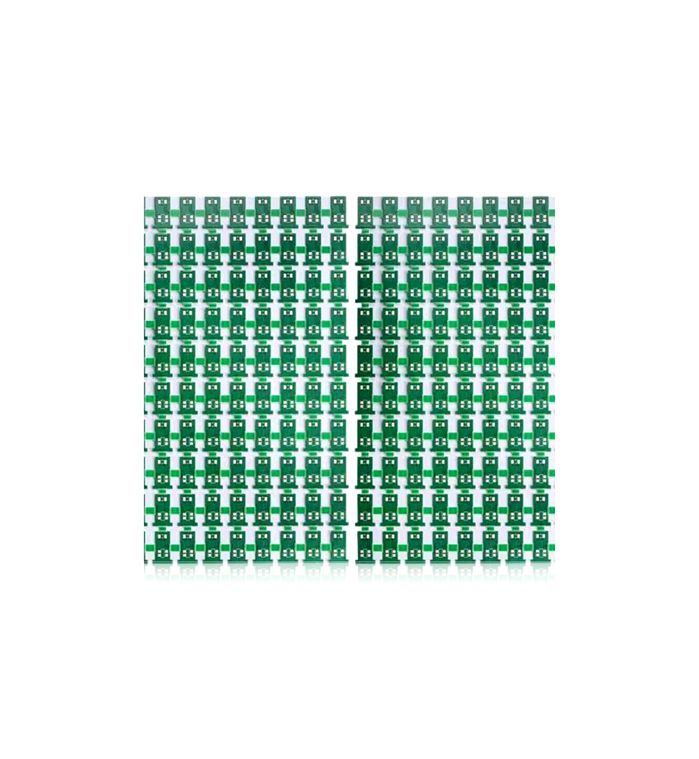
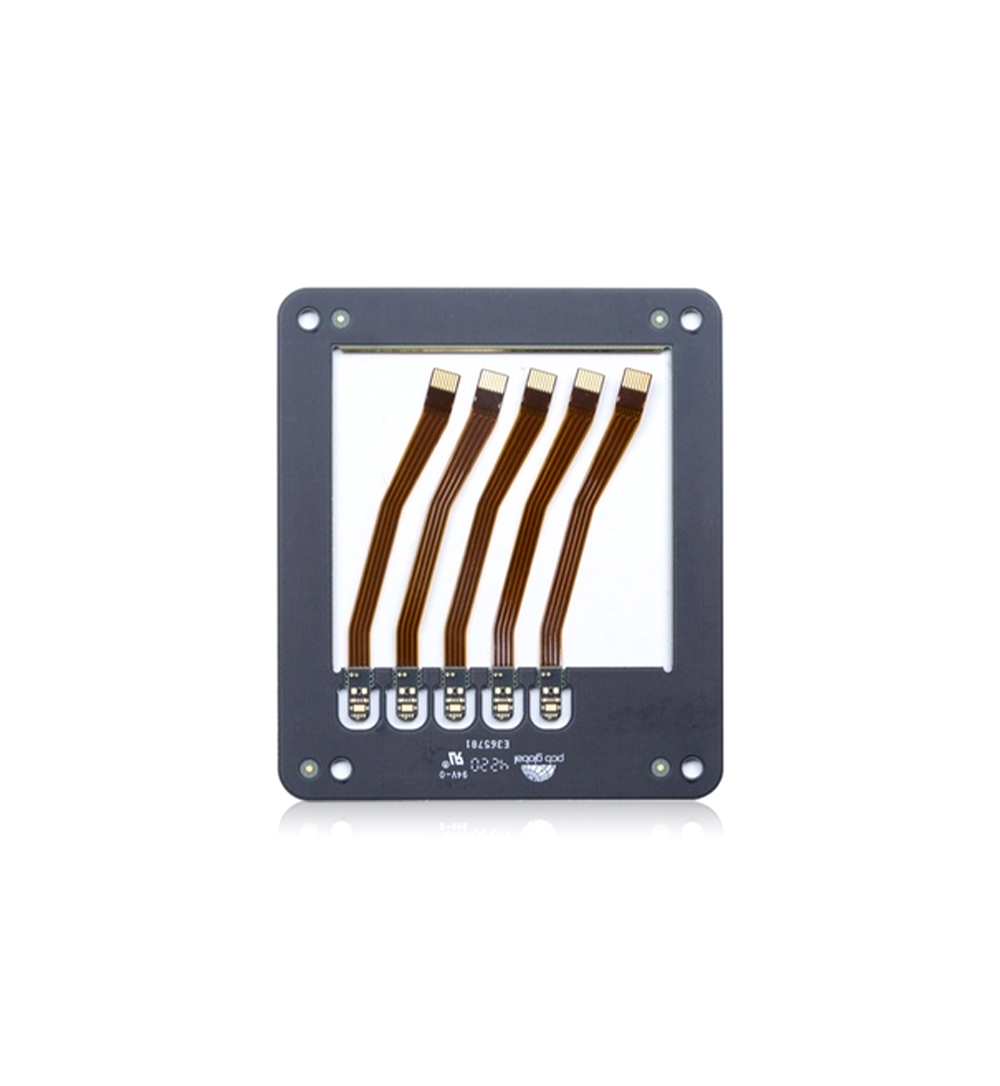
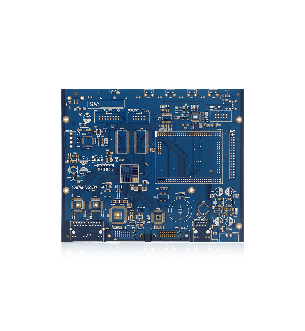
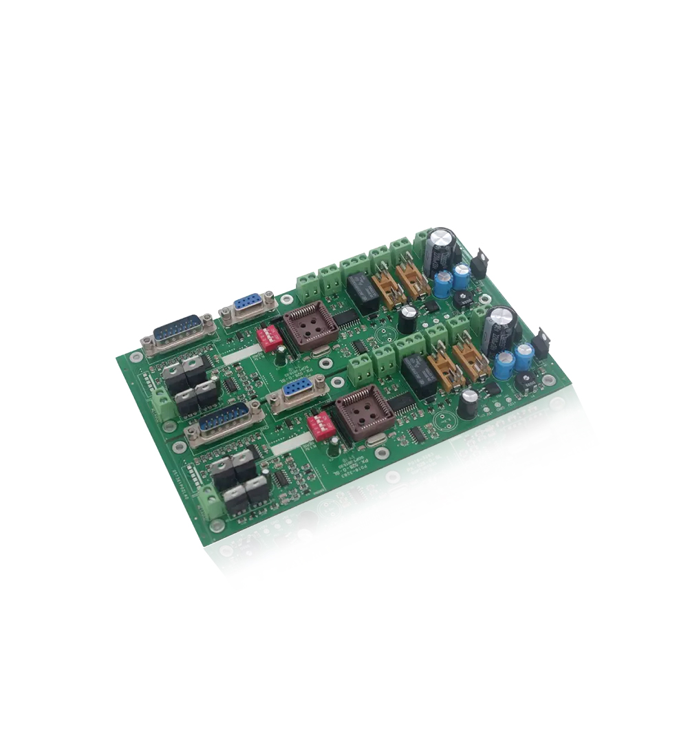
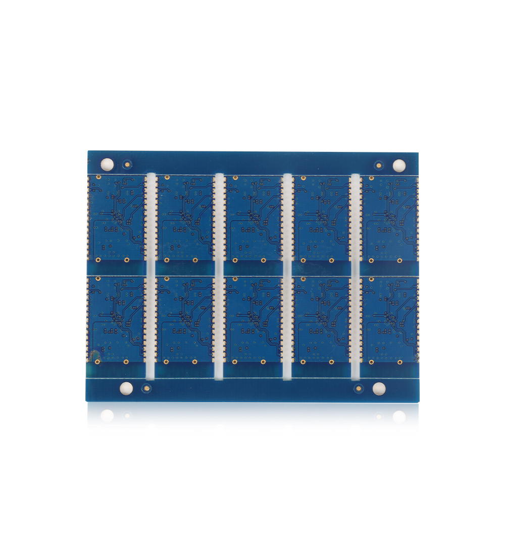
Multilayer pcb circuit board is a kind of printed circuit board, which is composed of alternating conductive graphic layers and insulating materials. The number of conductive patterns is more than three layers, and the electrical interconnection between layers is realized through metallized holes. If a double-sided circuit board is used as the inner layer, two single panels as the outer layer, or two double-sided boards as the inner layer, and two single panels as the outer layer, the conductive patterns are interconnected according to the design requirements by laminating the positioning system and insulating bonding materials, and then they become four layer, six layer, and eight layer circuit boards, also known as multilayer pcb circuit boards. As a professional PCB supplier, Shenzhen Zhongke Circuit Technology Co., Ltd. focuses on the production of high-precision double-sided/multi-layer PCB, high-order HDI boards, thick copper circuit boards, blind buried hole PCB boards, high-frequency circuit boards, PCB proofing and small and medium-sized batch boards.
Compared with the production process of general PCB multilayer boards and double-sided circuit boards, the main difference is that several unique process steps have been added to PCB multilayer boards: inner layer imaging and blackening, lamination, pitting and dirt removal. In most of the same processes, some process parameters, equipment accuracy and complexity are also different. For example, the inner layer metallization connection of the multilayer board is a decisive factor for the reliability of the multilayer board. The quality requirements for the hole wall are stricter than those for the double-layer board, so the requirements for drilling are higher. In addition, the number of laminated plates drilled each time, the drill speed and feed rate are different from those of the double panel. The inspection of finished products and semi-finished products of multilayer boards is more strict and complex than that of double-sided boards. Due to the complex structure of the multilayer board, the glycerol hot-melt process with uniform temperature should be used instead of the infrared hot-melt process that may lead to excessive local temperature rise.
① Remove oil stain, impurities and other pollutants on the surface;
② The oxidized surface is not affected by moisture at high temperature, reducing the probability of copper foil and resin delamination.
③ Make the non-polar copper surface become the surface with polar CuO and Cu2O, and increase the polar bond bonding between copper foil and resin;
④ Increasing the specific surface of the copper foil, thereby increasing the contact area with the resin, is conducive to the full diffusion of the resin and the formation of greater adhesion;
⑤ The boards made of the inner circuit must be blackened or browned before laminating. It is used to oxidize the circuit copper surface of the inner plate. Generally, the Cu2O generated is red and the CuO is black, so the Cu2O in the oxide layer mainly refers to browning and the CuO mainly refers to blackening.
Read recommendations:
1.5oz Multilayer Pcb Fabrication FR4 Printed Circuit Board Pcb 4 Layer
Welcome information, we will answer for you quickly

 No. 1 Jingtian Road, Xinsheng community, Longgang District, Shenzhen, Guangdong, China
 +86 13715096176
 Whatsapp/WeChat : +86 13715096176
 Kevin.kuang@xzgcircuits.com


 Return