source:Other information release time:2023-09-12 Hits: Popular:PCB Assembly company

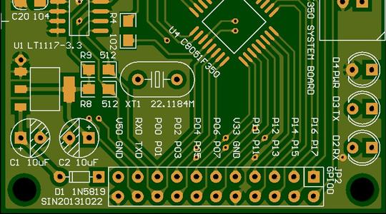
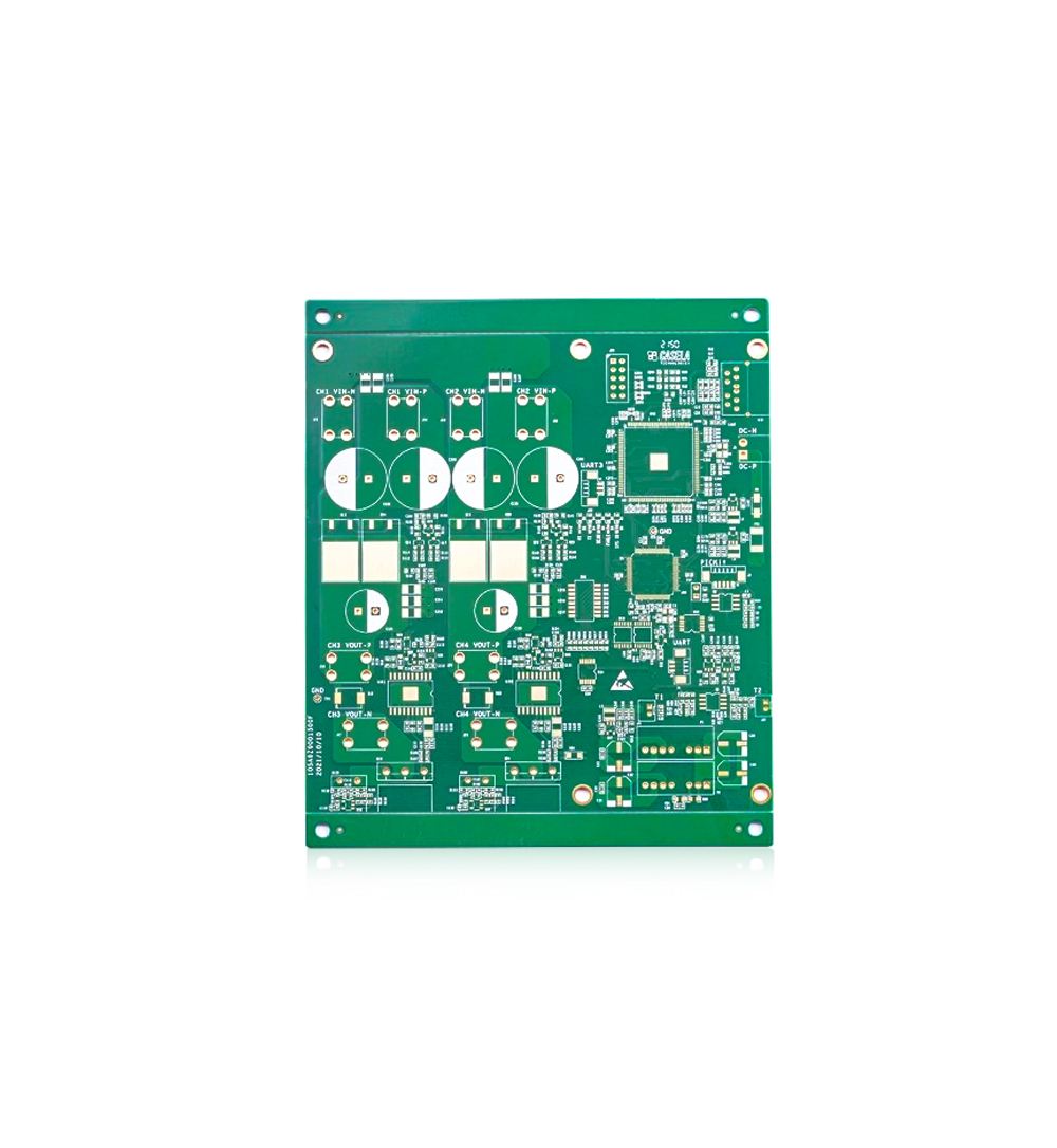
In PCB sampling, both gold deposition and gold plating are surface treatments. So, what are the advantages and disadvantages of the gold deposition and gold plating processes for PCB circuit boards?
Gold plating generally refers to "electroplated gold", "electroplated nickel gold", "electrolytic gold", etc. There is a distinction between soft gold and hard gold (usually hard gold is used for gold fingers). The principle is to dissolve nickel and gold (commonly known as gold salt) in chemical solution, immerse the circuit board in an electroplating cylinder, and connect the current to generate a nickel gold coating on the copper foil surface of the circuit board. Electroplated nickel gold has high hardness and is wear-resistant, The advantage of not being easily oxidized is widely used in electronic products.
Gold deposition is the process of generating a layer of coating through chemical oxidation-reduction reaction, which is generally thicker. It is one of the methods for depositing chemical nickel gold layers and can achieve a thicker gold layer.
The difference between sinking gold and gilding:
1. The crystal structure formed by gold deposition is different from that of gold plating. The thickness of gold deposited by gold deposition is much thicker than that of gold plating, and it will appear golden yellow, which is one of the methods to distinguish between gold plating and gold deposition.
2. Sinking gold is easier to weld than plating gold, and it will not cause poor welding.
3. The solder pad of the sinking gold plate only has nickel gold, and the skin effect of the signal is transmitted on the copper layer without affecting the signal.
4. The crystal structure of precipitated gold is denser than that of plated gold, and it is less prone to oxidation.
5. Plating can easily short-circuit the gold wire. And the solder pad of the sinking gold plate only has nickel gold, so there will be no gold wire short circuit.
6. The solder pad of the sinking gold plate only has nickel gold, so the connection between the wire resistance and the copper layer is more solid.
7. The flatness and service life of the gold plated plate are better than those of the gold plated plate.
Read recommendations:
Blue Solder Mask Double Sided PCB Board High TG TG170 S1000-2
Welcome information, we will answer for you quickly

 No. 1 Jingtian Road, Xinsheng community, Longgang District, Shenzhen, Guangdong, China
 +86 13715096176
 Whatsapp/WeChat : +86 13715096176
 Kevin.kuang@xzgcircuits.com


 Return