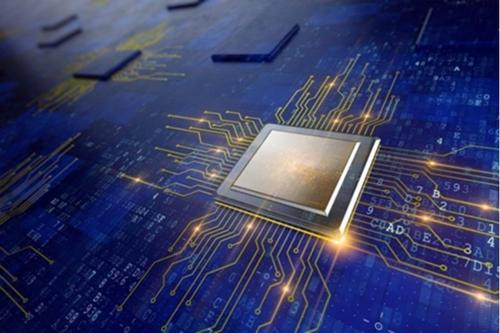
source:Other information release time:2023-09-05 Hits: Popular:PCB Assembly company
Through holes are the most common holes in PCB circuit boards, mainly playing a role in connecting and conducting circuits. Next, let the engineer share with you the classification of PCB through-holes.
Through holes are traditionally divided into electroplated (supported) holes and non electroplated (unsupported) holes. This is a manufacturing term, and for design purposes, holes should be divided into two categories: welded and unwelded.
1. Welded through holes.
Most rules apply to welded through holes, except that the outer surface area must be large to enhance heat dissipation and avoid welding defects. For consistency and ease of calculation, unless simplified pads are required, the inner pad should be the same as the outer pad
2. A through hole that is not welded.
The designer must first know whether the solder pad is confirmed to be welded or not. This information helps engineers decide whether the calculation of the solder pad is for welding or for the minimum orifice ring. It should be noted that the solder pads are electroplated or not charged. During the electroplating process, if the solder pads exist, the holes need to be plated with copper foil. If the solder pad is not electroplated, it must be drilled after the electroplating process.
(1) Non plated through holes with solder pads
Non plated through holes refer to holes that pass through the solder pad without plating. This means that there is no additional carrier to support the solder pad in addition to the normal copper adhesive. For this reason, the solder pad must be large enough to facilitate adhesion and support during heating or welding.
(2) Non plated through hole, no solder pad
Universal NPTH is the same size as a non solder pad or hole wall electroplated hole on a printed board, such as installation holes, screw adjustment access holes, wire transfer holes, etc. Non electroplating or ring requirements are necessary, and universal through-holes are different from other holes as they do not require electroplating or soldering considerations.
Read recommendations:
Welcome information, we will answer for you quickly

 No. 1 Jingtian Road, Xinsheng community, Longgang District, Shenzhen, Guangdong, China
 +86 13715096176
 Whatsapp/WeChat : +86 13715096176
 Kevin.kuang@xzgcircuits.com


 Return