source:Other information release time:2023-04-08 Hits: Popular:PCB Assembly company

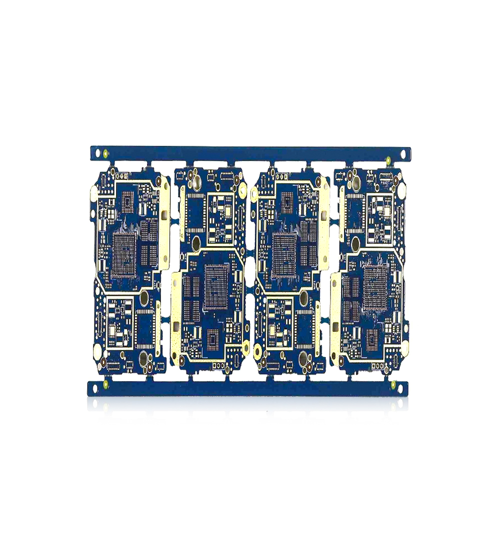
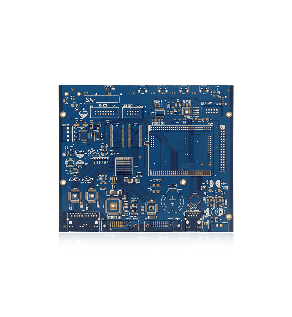
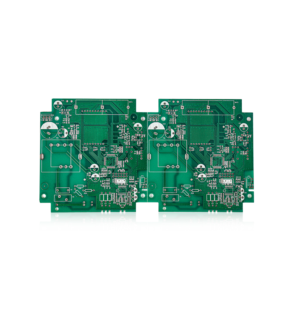
The designer may design a strange number layer printed circuit board (PCB). If the wiring does not require an extra layer, why should it be used? Is the reduction layer not to make the circuit board thinner? If the circuit board is one less layer, isn't the cost? The layer will reduce the cost.
The circuit board has two different structures: nuclear core structure and foil structure.
In the nuclear core structure, all the conductive layers in the circuit board are applied to the nuclear core material; in the foil structure, only the internal conductive layer of the circuit board is applied to the nuclear core material. All conductive layers are bonded together through a multi -layer pressure process through the medium.
Nuclear materials are the double -sided foil in the factory. Because each nucleus has two places, the number of conductivity layers of PCB is even when comprehensive use. Why not use foil and the rest of the nuclear structure? The main reason is: the cost of PCB and the curvature of PCB.
The cost advantage of the even layer circuit board
Because one less layer of medium and foil, the cost of the raw material of the PCB board is slightly lower than that of the even -layer PCB. However, the processing cost of the odd number layer PCB is significantly higher than that of the even -layer PCB. The processing cost of the inner layer is the same; but the applied foil/nuclear structure significantly increases the treatment cost of the outer layer.
The PCB of the odd layer needs to increase the non -standard layer of layer bonding process on the basis of the nuclear structure process. Compared with nuclear structures, the production efficiency of factory production in the nuclear structure will decline. Before the layer pressure bonding, the outer nucleus requires additional process treatment, which increases the risk of scratching and etching errors in the outer layer.
Balanced structure Avoid bending
The best reason for designing PCB without the odd number layer is: the strange number layer circuit board is easy to bend. When the PCB is cooled after the multi -layer circuit bonding process, different layer of pressure tension when the nuclear structure and the foil structure are cooling can cause PCB to bend. As the thickness of the circuit board increases, the greater the risk of composite PCB with two different structures. The key to eliminating circuit boards is to use balanced layers. Although the bending PCB meets the standard requirements, the subsequent processing efficiency will be reduced, resulting in increased costs. Because special equipment and processes are required during assembly, and the accuracy of components is reduced, the quality of damage is reduced.
Read recommendations:
Multilayer Printed Circuit Board 1OZ 4 Layer Multilayer Pcb FR4 TG170 Blue Solder Mask
1.6mm HASL OSP Multi Layer Pcb Board FR4 Halogen Free Green Solder Mask
Welcome information, we will answer for you quickly

 No. 1 Jingtian Road, Xinsheng community, Longgang District, Shenzhen, Guangdong, China
 +86 13715096176
 Whatsapp/WeChat : +86 13715096176
 Kevin.kuang@xzgcircuits.com


 Return