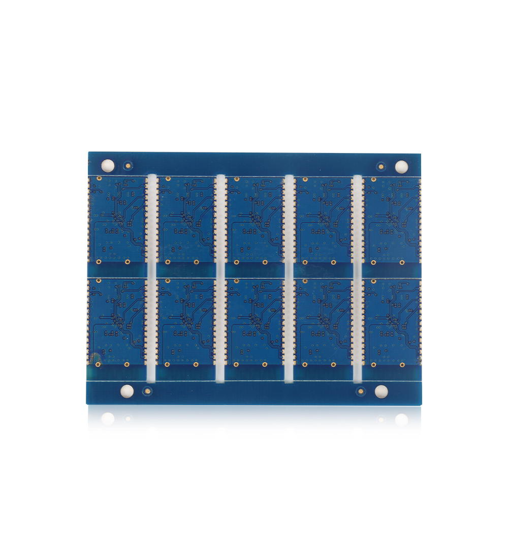
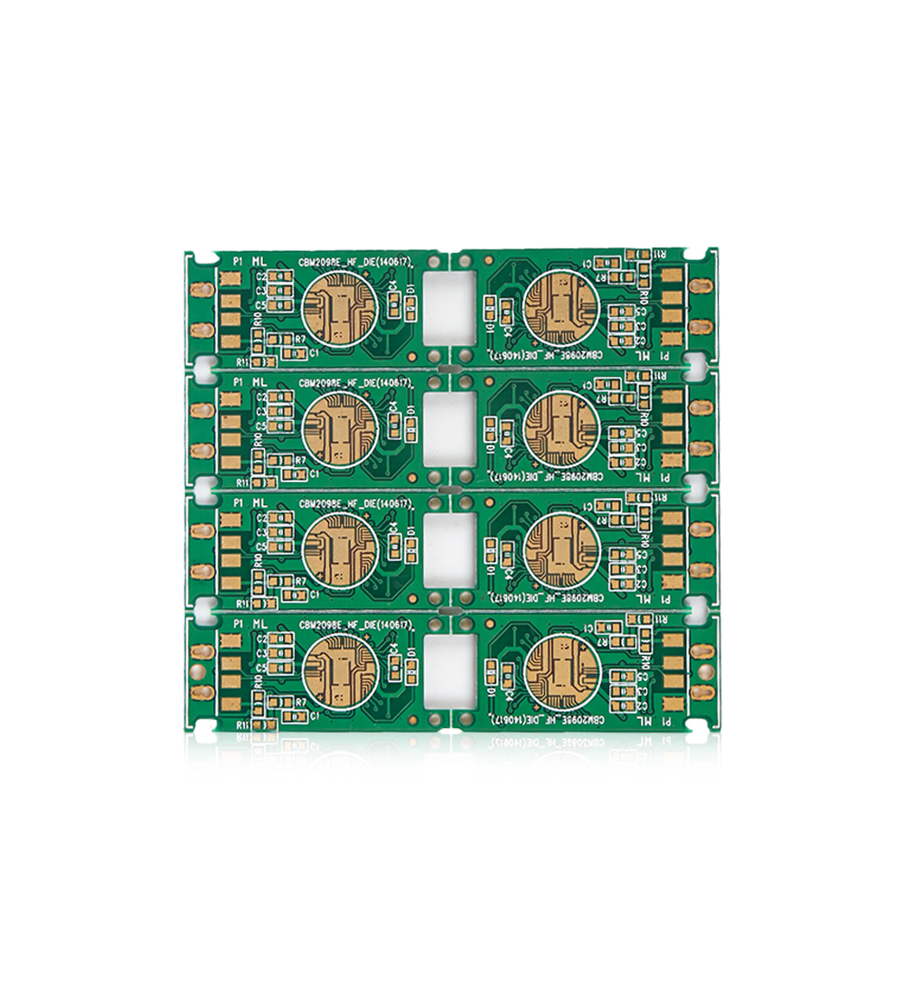
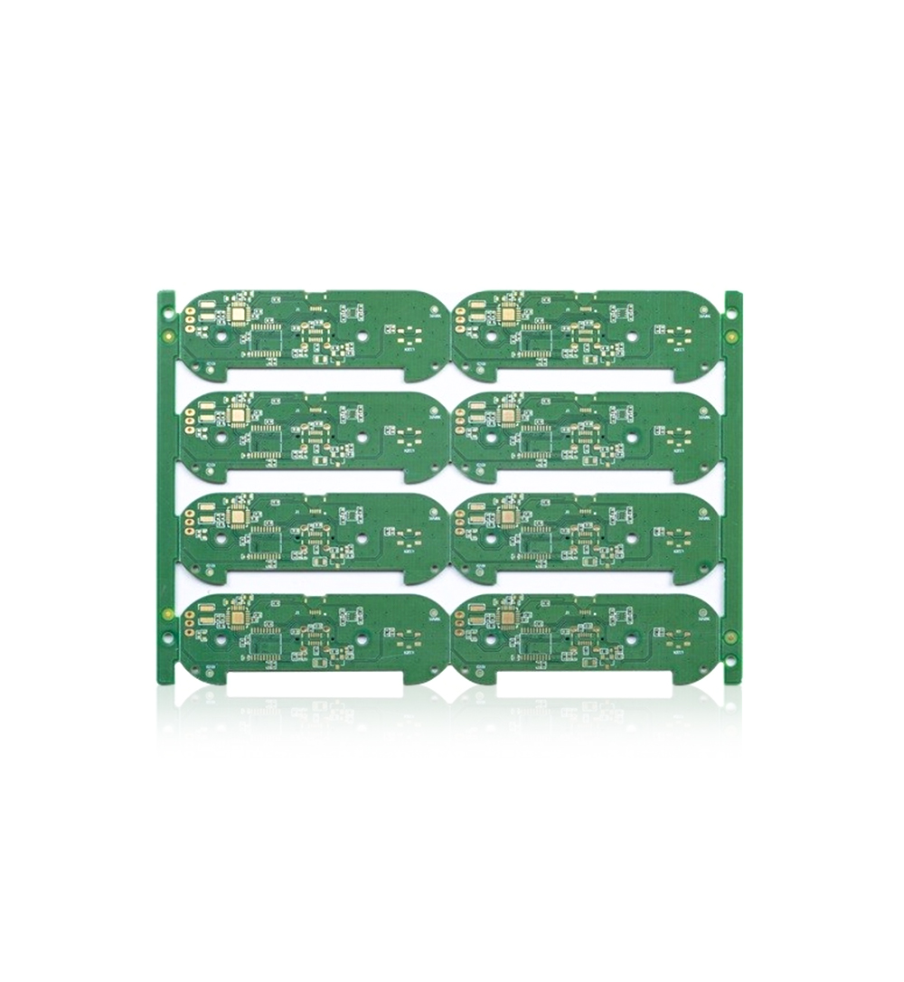
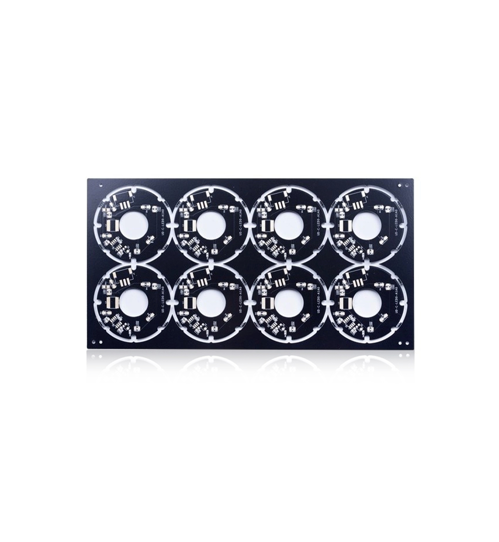
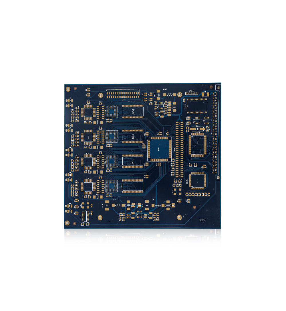
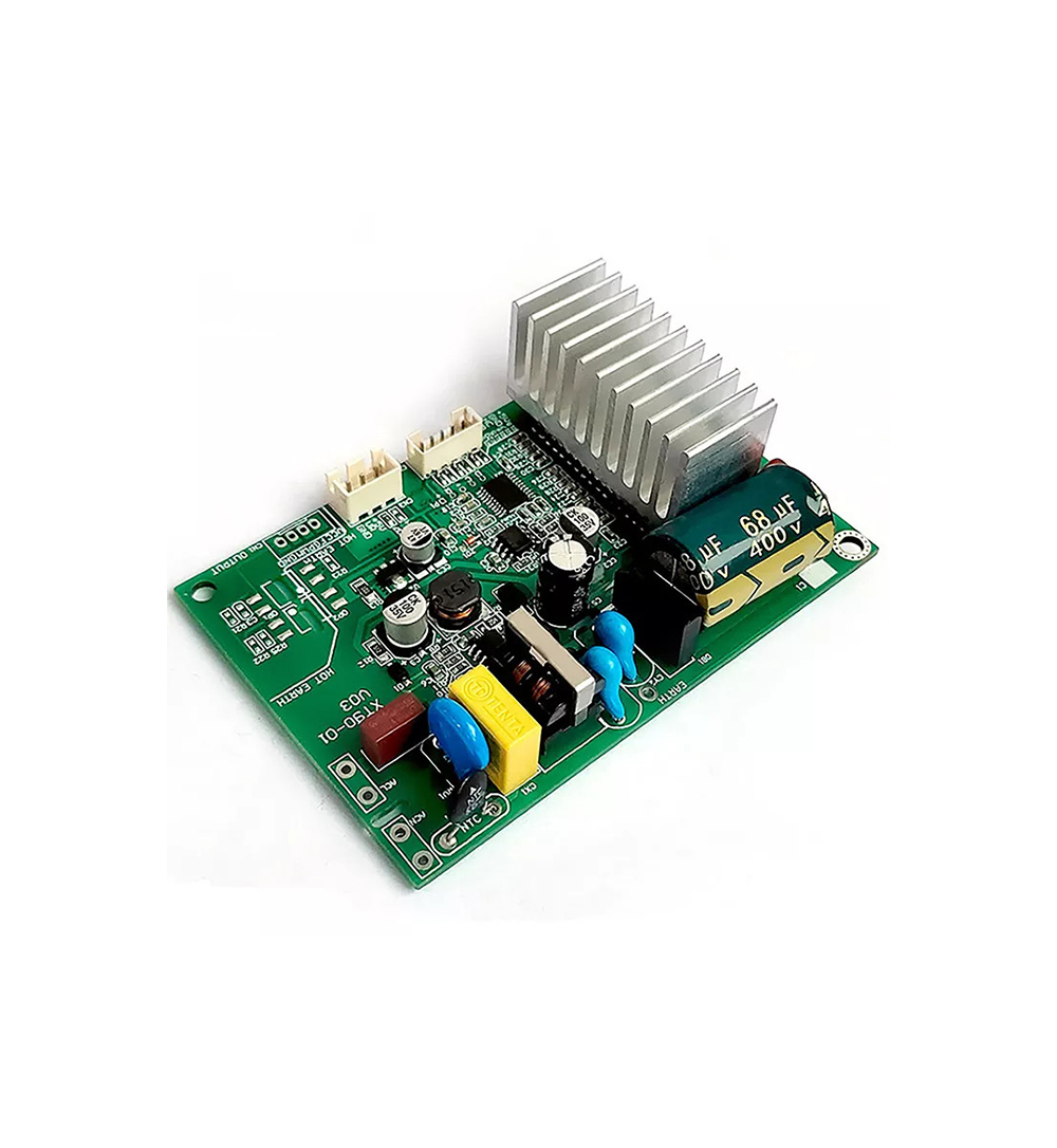
source:Other information release time:2023-03-09 Hits: Popular:PCB Assembly company

1) For PCB with a non -transmitted edge size greater than 300mm, the heavier devices should not be arranged in the middle of the PCB to reduce the impact of the weight of the PCB deformation during the welding process due to the weight of the inserted device, and the installation process on the board on the board. The influence of the latter device.
2) For the convenience of installation, the device is recommended to be arranged near the installation operation side.
3) The length of the length of the device with a long size (such as memory strip sockets, etc.) is consistent with the direction of transmission.
4) The distance between the edge of the pile of the pile and the pitch ≤ 0.65mm of the pads of the pile of the pilot backwalm device is greater than 20mm between the QFP, SOP, connectors and all BGAs. The distance from other SMT devices is> 2mm.
5) The distance between the body of the pilot return welding device is> 10mm.
6) The distance between the edge of the pile of the pile of the pile of the pilot and the transmission is ≥10mm;
Read recommendations:
Welcome information, we will answer for you quickly

 No. 1 Jingtian Road, Xinsheng community, Longgang District, Shenzhen, Guangdong, China
 +86 13715096176
 Whatsapp/WeChat : +86 13715096176
 Kevin.kuang@xzgcircuits.com


 Return