source:Other information release time:2023-08-02 Hits: Popular:PCB Assembly company

ENIG, also known as nickel immersion gold plating, is one of the surface treatment processes for PCBs. It has advantages such as high flatness, low contact resistance, wear resistance, good heat resistance, and long storage time. It combines the advantages of weldability, touchability, wiring ability, and heat dissipation. It has a position that cannot be replaced by other surface treatments and is the preferred choice for high-end PCB surface treatment processes.
There is no perfect thing in the world, there are always advantages and disadvantages. The surface treatment process of nickel plating and gold immersion is no exception, and this drawback is also quite fatal. That's the black mat.
The most fatal thing is that the appearance of black pads is relatively hidden, with a perfect and flawless appearance, but in reality, it implies a "killing machine". Once it occurs, it will affect the strength of the solder joints, thereby affecting the welding quality of PCBA components after assembly. However, this is also an occasional small probability event.
Below, we will explore the causes of black mats and some measures to avoid them.
Based on relevant research data and results, the reasons for the occurrence of black mats are as follows.
1) In the Single displacement reaction, when a small nickel atom is oxidized and dissolved, two large gold atoms will be reduced and deposited at the same time. When the lattice grows, it will result in a fully pushing differential displacement Misaligence, so that there are many voids and pores in the interface between nickel and gold, and even liquid medicine is hidden, which is easy to cause continued passivation and oxidation of the nickel surface.
2) In the Single displacement reaction, the gold liquid is excessively active and contains more phosphorus, which not only produces black pad but also affects the strength of solder joints.
3) Poor management of nickel chemical solution and insufficient hardening of green paint.
4) If the thickness of the replacement gold layer is too thick, especially if it exceeds 5 inches, the thick gold layer will cause strong attack on the self nickel layer. This is the main reason for the formation of black mats.
Read recommendations:
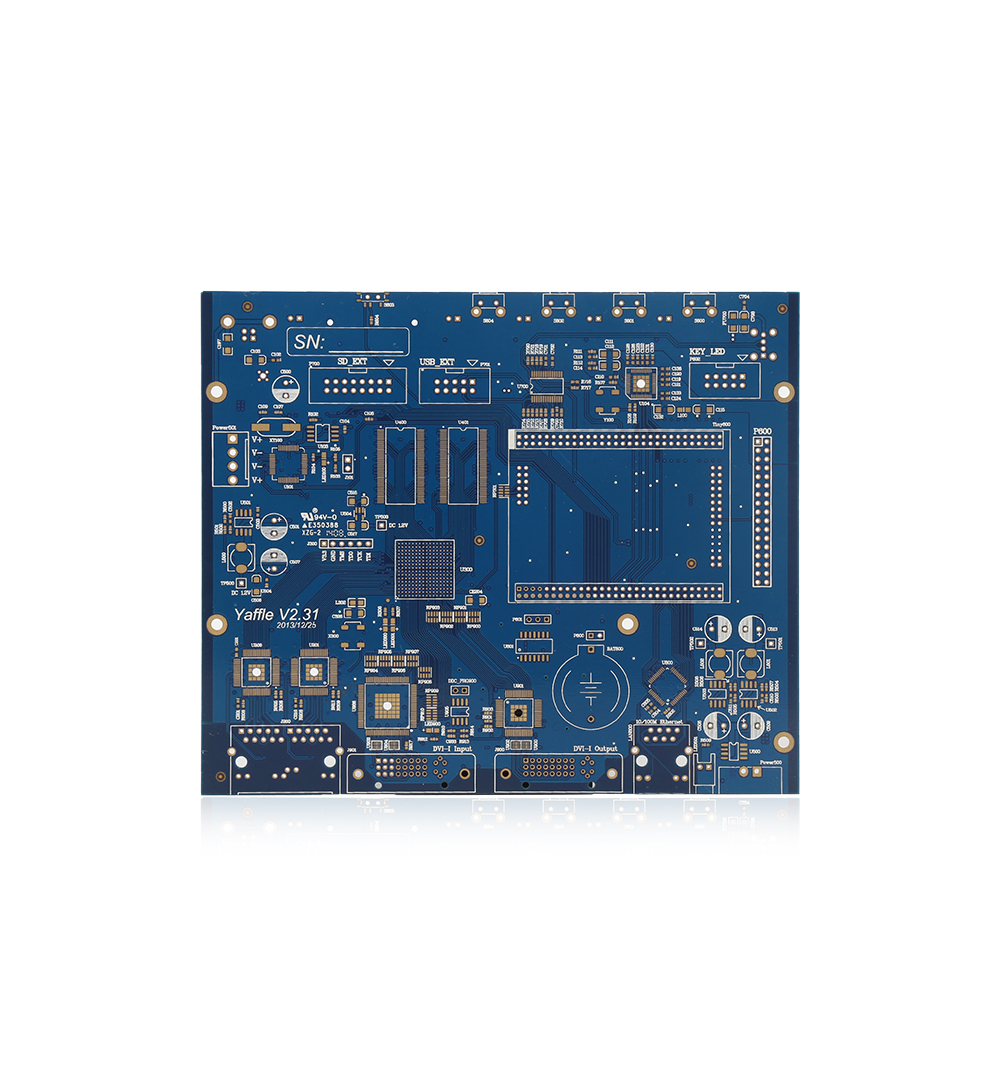
Blue Solder Mask Double Sided PCB Board High TG TG170 S1000-2
Welcome information, we will answer for you quickly

 No. 1 Jingtian Road, Xinsheng community, Longgang District, Shenzhen, Guangdong, China
 +86 13715096176
 Whatsapp/WeChat : +86 13715096176
 Kevin.kuang@xzgcircuits.com


 Return