source:Other information release time:2023-09-09 Hits: Popular:PCB Assembly company

1. The effect of reducing temperature on the stress of PCB circuit boards
Since temperature is the main source of stress on circuit boards, reducing the temperature of the reflow furnace or slowing down the heating and cooling rate of circuit board production in the reflow furnace can greatly reduce the occurrence of board bending and warping. However, there may be other side effects, such as solder short circuits.
2. PCB adopts high Tg board
Tg is the glass transition temperature, which is the temperature at which a material transitions from a glass state to a rubber state. The lower the Tg value of a material, the faster its circuit board begins to soften after entering the reflow furnace, and the longer it takes to become a soft rubber state, the more severe the deformation of the circuit board. The use of boards with higher Tg can increase their ability to withstand stress and deformation, but the cost of materials used in circuit board production is also relatively high.
3. Increase the thickness of the PCB circuit board
Many electronic products, in order to achieve the goal of being lighter and thinner, have left a thickness of 1.0mm, 0.8mm, or even 0.6mm on the circuit board. This thickness is a bit difficult to maintain when the circuit board is not deformed after being soldered in the reflow furnace. It is recommended that if there is no requirement for lightness, it is best to use a thickness of 1.6mm on the circuit board, which can greatly reduce the risk of bending and deformation.
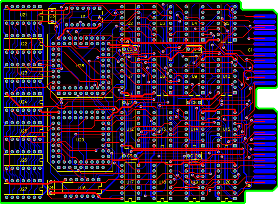
4. Reduce the size of circuit boards and the number of splices
Since most reflow furnaces use chains to drive the circuit board forward, the larger the PCB design size, the more concave and deformed the circuit board will be in the reflow furnace due to its own weight. Therefore, try to place the long side of the circuit board as the board edge on the chain of the reflow furnace to reduce the concave deformation caused by the weight of the circuit board itself. The reduction in the number of splicing boards is also based on this reason, that is, when it comes to the furnace, Try to use narrow edges perpendicular to the direction of the furnace to achieve the lowest amount of concave deformation.
Read recommendations:
Metal Core 0.8mm Led Street Light Pcb Aluminium Pcb Board For Led
Welcome information, we will answer for you quickly

 No. 1 Jingtian Road, Xinsheng community, Longgang District, Shenzhen, Guangdong, China
 +86 13715096176
 Whatsapp/WeChat : +86 13715096176
 Kevin.kuang@xzgcircuits.com


 Return