source:Other information release time:2023-02-08 Hits: Popular:PCB Assembly company

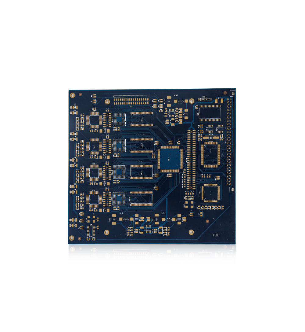
1. Selection of the width of the printing wire: The minimum width of the printing wire is related to the current flow of the flowing wire: PCB board width is too small, the resistance of the rigid printing wire is large, and the voltage on the line is large. , The width is too wide, the wiring density is not high, and the area of the PCB board increases. In addition to increasing the cost, it is not conducive to miniaturization. If the current load is calculated at 20A/square millimeter, when the thickness of the copper foil is 0.5mm, (generally (generally For so many,) The current load of 1mm (about 40mil) line width is 1A. Therefore, the line width is 1–2.54mm (40–100mil) can meet the general application requirements. The ground wires and power supply on the high -power device board board board According to the power size, the wire width can be appropriately increased, and in the small power digital circuit, in order to increase the wiring density, the minimum line width is 0.254–1.27mm (10–15mil). In the same circuit board, the power line.
2. The pitch of the PCB board: When it is 1.5mm (about 60mil), the insulation resistance of the lines between the lines is greater than 20m Euros, the maximum resistance of the line between the line can reach 300V. The voltage is 200V, so on the circuit board with low voltage (between line voltage is not greater than 200V), the wire spacing is 1.0–1.5mm (40-60mil) in the low-voltage circuit, such as the digital circuit system, there is no need to consider the breakdown voltage. As long as the production process allows, it can be small.
3. Pad pad: For the resistance of 1/8W, the diameter of the pads is 28mil. For 1/2W, the diameter is 32mil, the lead hole is too large, and the width of the copper ring ring of the pads is relatively reduced. , Resulting in the decline of the attachment of the pad. It is easy to fall off, the lead hole is too small, and the component is difficult to install.
4. Circuit frame of the circuit board: The shortest distance between the border line and the component pin pad should not be less than 2mm, (generally 5mm more reasonable), otherwise it is difficult to get.
5. Principles of component layout:
A. General principles: In the design of the PCB board, if the circuit system exists at the same time digital circuit and analog circuit. And large current circuits, the layout must be separated to minimize the crickets between each system. And function, block, partitioning component.
B. Component placement direction: The component can only be arranged in the horizontal and vertical directions. Otherwise, it is not allowed to be in the plug -in.
C. When the difference between the parts of the component is large, the component spacing should be large enough to prevent discharge.
D. Input signal processing unit, the output signal driving element should be close to the circuit board, so that the input and output signal line should be as short as possible to reduce the interference of the input and output.
Read recommendations:
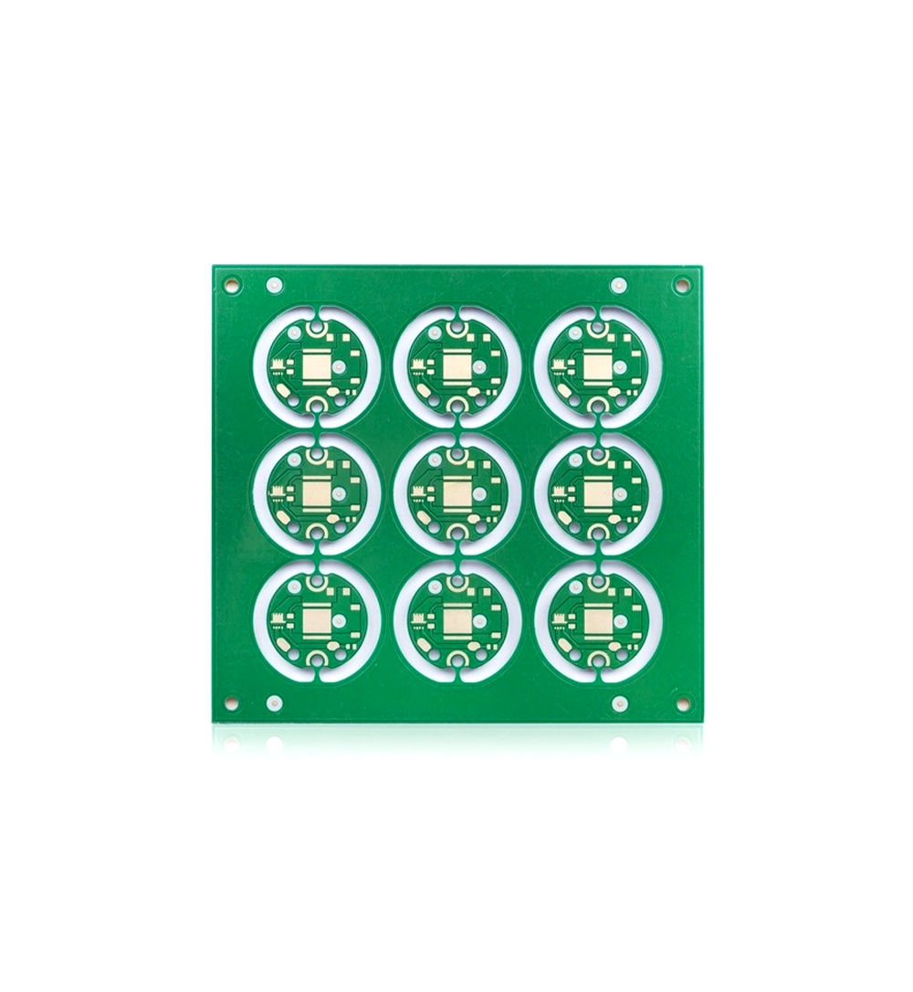
Metal Core 0.8mm Led Street Light Pcb Aluminium Pcb Board For Led
PI FR4 Double Layer Flex PCB Board Immersion Gold 2L Lightweight
FR4 TG170 Rigid Flex PCB Fabrication Immersion Gold Green Color Solder Mask
Welcome information, we will answer for you quickly

 No. 1 Jingtian Road, Xinsheng community, Longgang District, Shenzhen, Guangdong, China
 +86 13715096176
 Whatsapp/WeChat : +86 13715096176
 Kevin.kuang@xzgcircuits.com


 Return