source:News release time:2023-08-11 Hits: Popular:PCB Assembly company
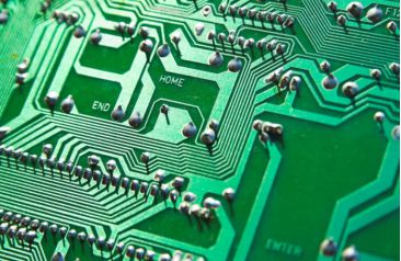
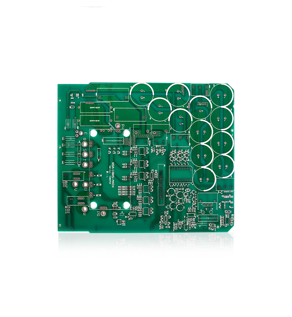
PCB circuit board printing mainly passes through equipment, solder pads, vias, wiring, silk screen printing, and solder mask positioning holes in the process flow.
Equipment (Part): Meta equipment welded onto a PCB board, which is also the effect of the PCB. The equipment is presented on a PCB optical board using a pad+screen printing method
Pad: Connect the pins of the meta equipment to the board through electrical methods, which correspond to the pins of the equipment
Track/Trace: The signal line connecting the pins of the equipment depends on the nature of the signal, such as current size, speed, etc. The length and width of the line also vary
Via: If the circuit cannot complete all signal wiring at one level, it needs to be connected across layers through via. The method and aperture of via depend on the characteristics of the signal and the requirements of the processing plant's process
Layer - The circuit board is divided into many layers, in addition to the signal layer, there are other layers used to define processing purposes, etc
Silk screen/overlay: also known as silk screen layer, used to label various relevant information on equipment
Solder mask: A protective layer that can be understood literally to prevent adjacent pins without electrical connection from being accidentally soldered
Mounting hole: a hole placed for ease of installation or debugging
Read recommendations:
Welcome information, we will answer for you quickly

 No. 1 Jingtian Road, Xinsheng community, Longgang District, Shenzhen, Guangdong, China
 +86 13715096176
 Whatsapp/WeChat : +86 13715096176
 Kevin.kuang@xzgcircuits.com


 Return