source:News release time:2023-09-11 Hits: Popular:PCB Assembly company
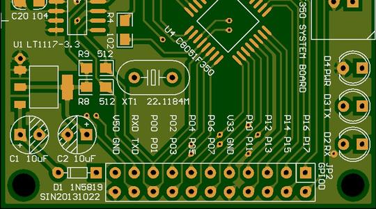
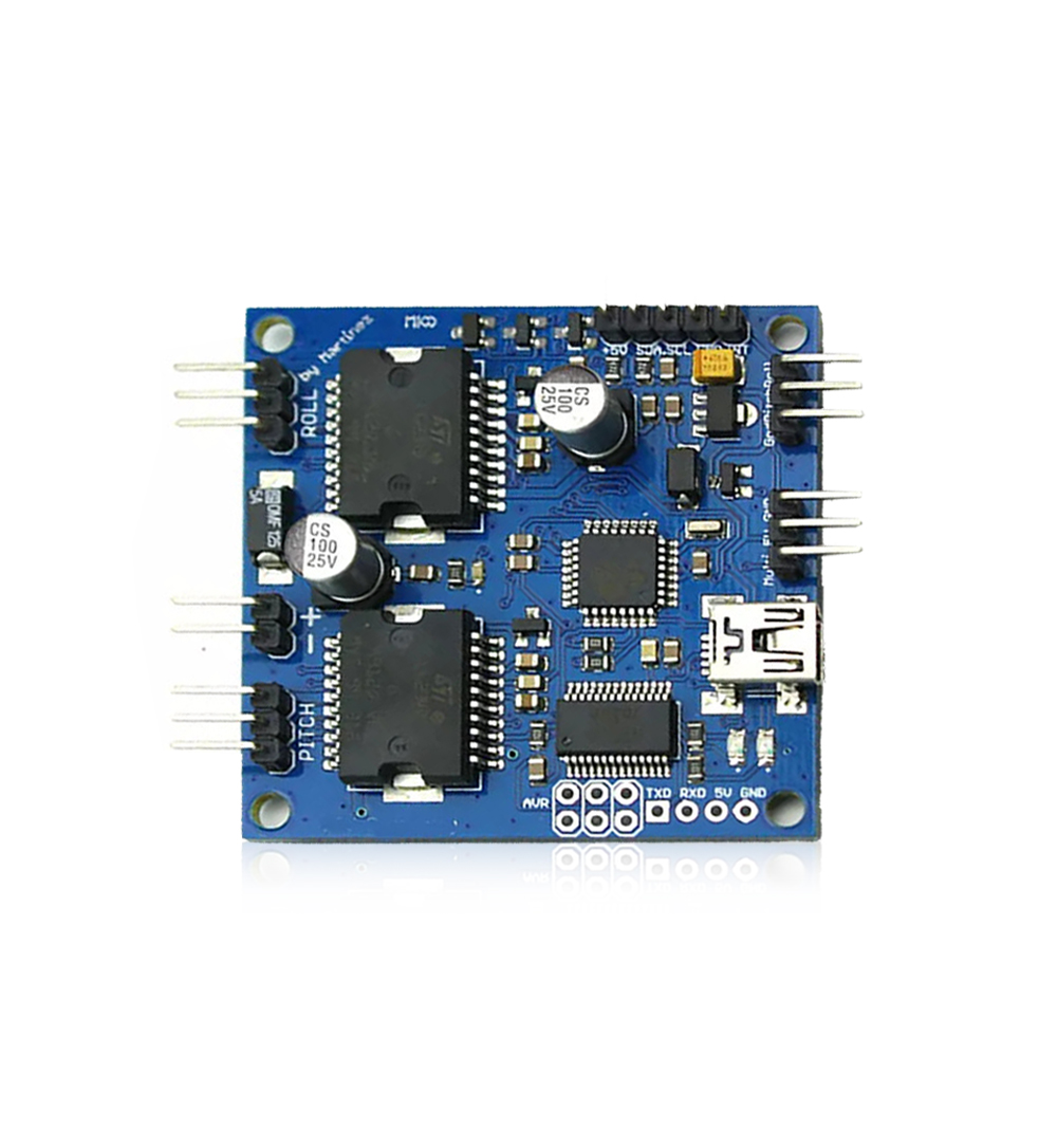
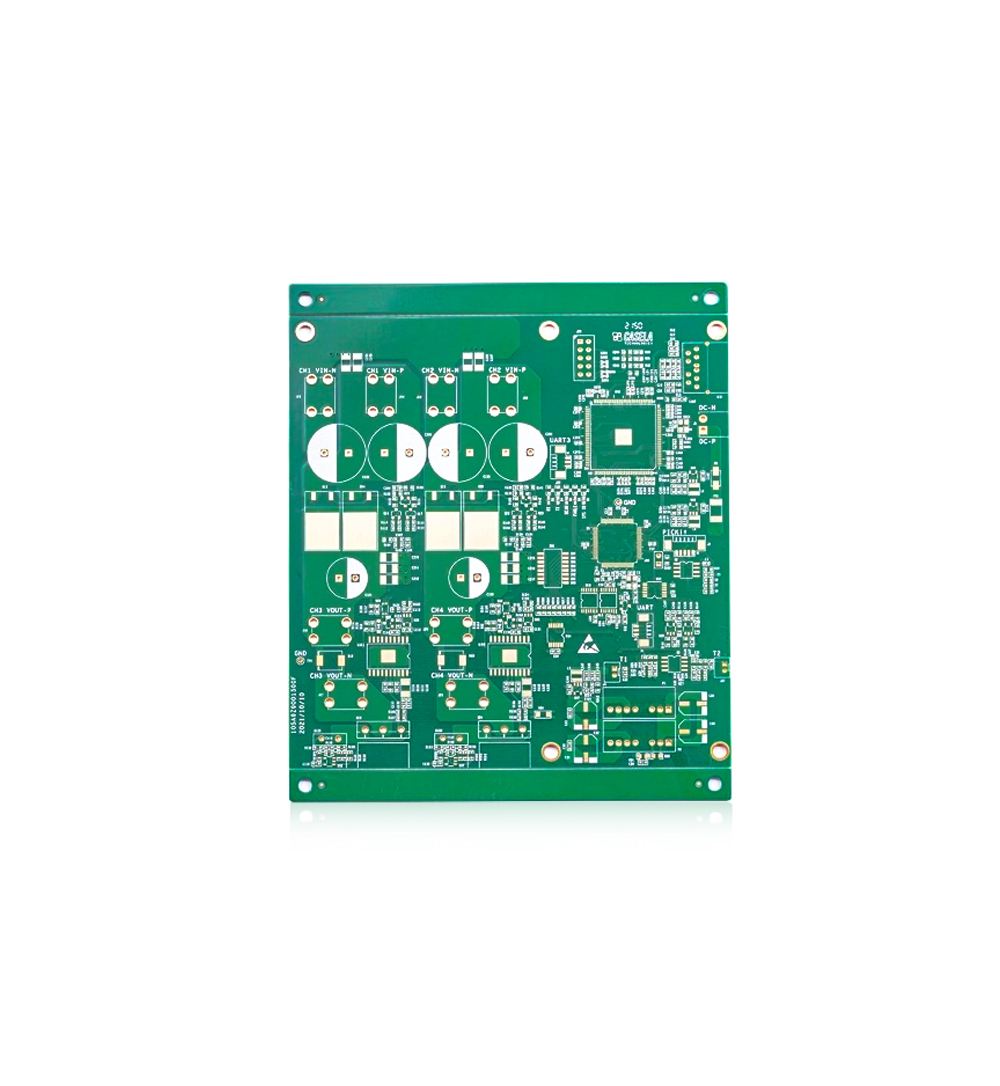
Through holes (via) are an important component of multi-layer PCBs. Simply put, each hole on a PCB can be referred to as a through hole. From the perspective of function, vias can be divided into two categories: one is used as electrical connections between layers; The second is used for fixing or positioning devices. If viewed from a process perspective, vias are generally divided into three categories, namely blind holes, buried holes, and through holes. So, what are the techniques for designing through holes in PCB circuit boards?
1. Considering both cost and signal quality, choose a reasonable size of the via hole. For example, for the PCB design of memory modules with 6-10 layers, it is better to use 10/20Mil (drilled/soldered) through holes. For some high-density small-sized boards, it is also possible to try using 8/18Mil through holes. Under current technical conditions, it is difficult to use smaller sized vias. For the via of the power or ground wire, larger sizes can be considered to reduce impedance.
2. The via itself has parasitic capacitance to the ground, which can prolong the signal rise time and reduce the circuit speed; At the same time, there is also parasitic inductance in the via, which weakens the contribution of the bypass capacitor and weakens the filtering effectiveness of the power system. Therefore, when designing vias, it is necessary to consider using thinner PCB boards, which helps to reduce the two parasitic parameters of vias.
3. The signal wiring on the PCB board should not be changed layers as much as possible, which means that unnecessary vias should not be used as much as possible.
4. The pins of the power supply and ground should be perforated nearby, and the shorter the lead between the vias and pins, the better, as they can lead to an increase in inductance; At the same time, the power and ground leads should be as thick as possible to reduce impedance.
Read recommendations:
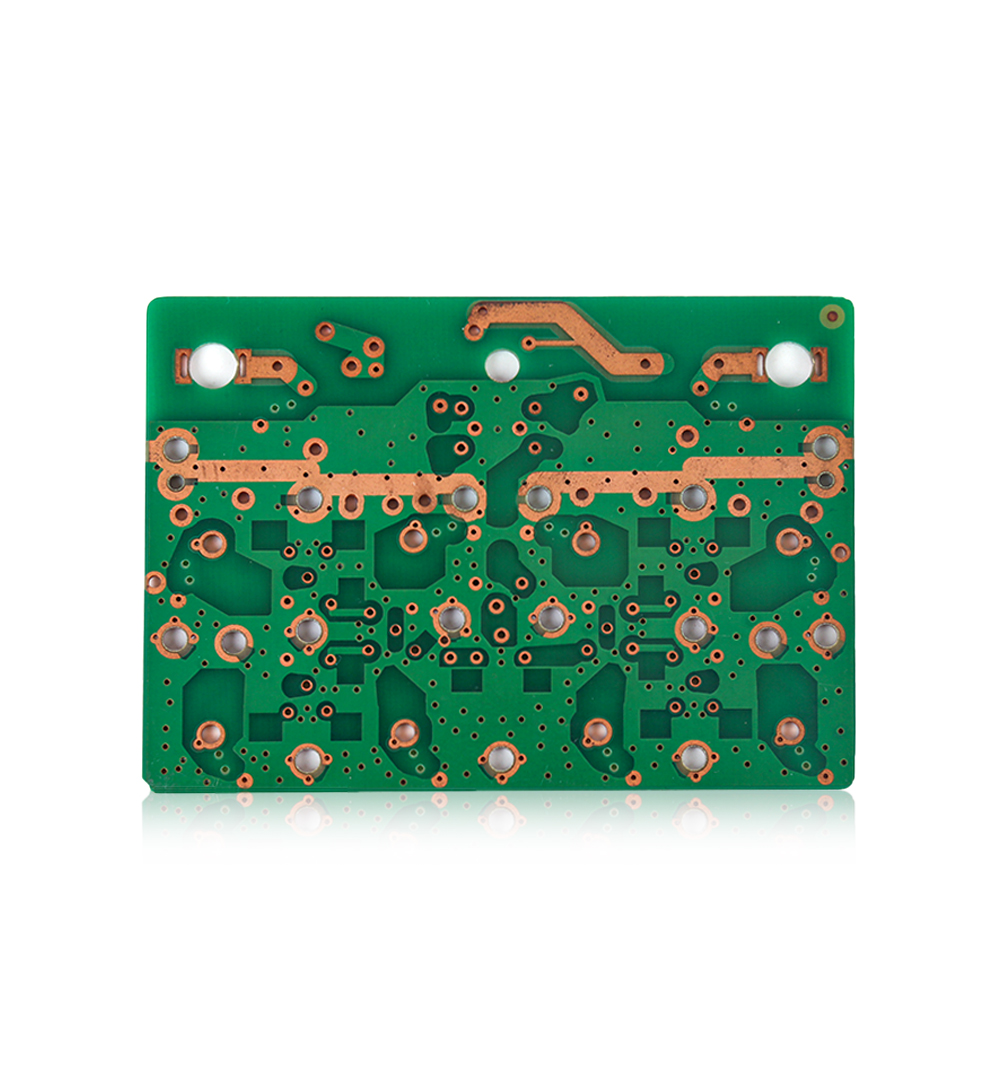
TG150 Halogen Free Fr4 PCB Board Double Sided 1.6mm 6mil Immersion Gold
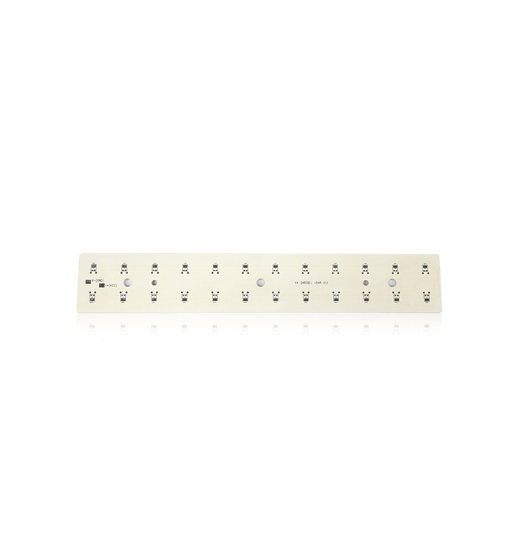
Metal Core 0.8mm Led Street Light Pcb Aluminium Pcb Board For Led
Welcome information, we will answer for you quickly

 No. 1 Jingtian Road, Xinsheng community, Longgang District, Shenzhen, Guangdong, China
 +86 13715096176
 Whatsapp/WeChat : +86 13715096176
 Kevin.kuang@xzgcircuits.com


 Return