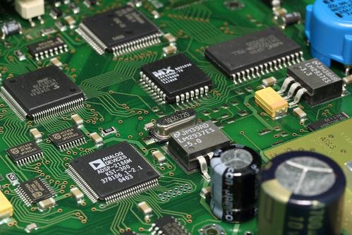
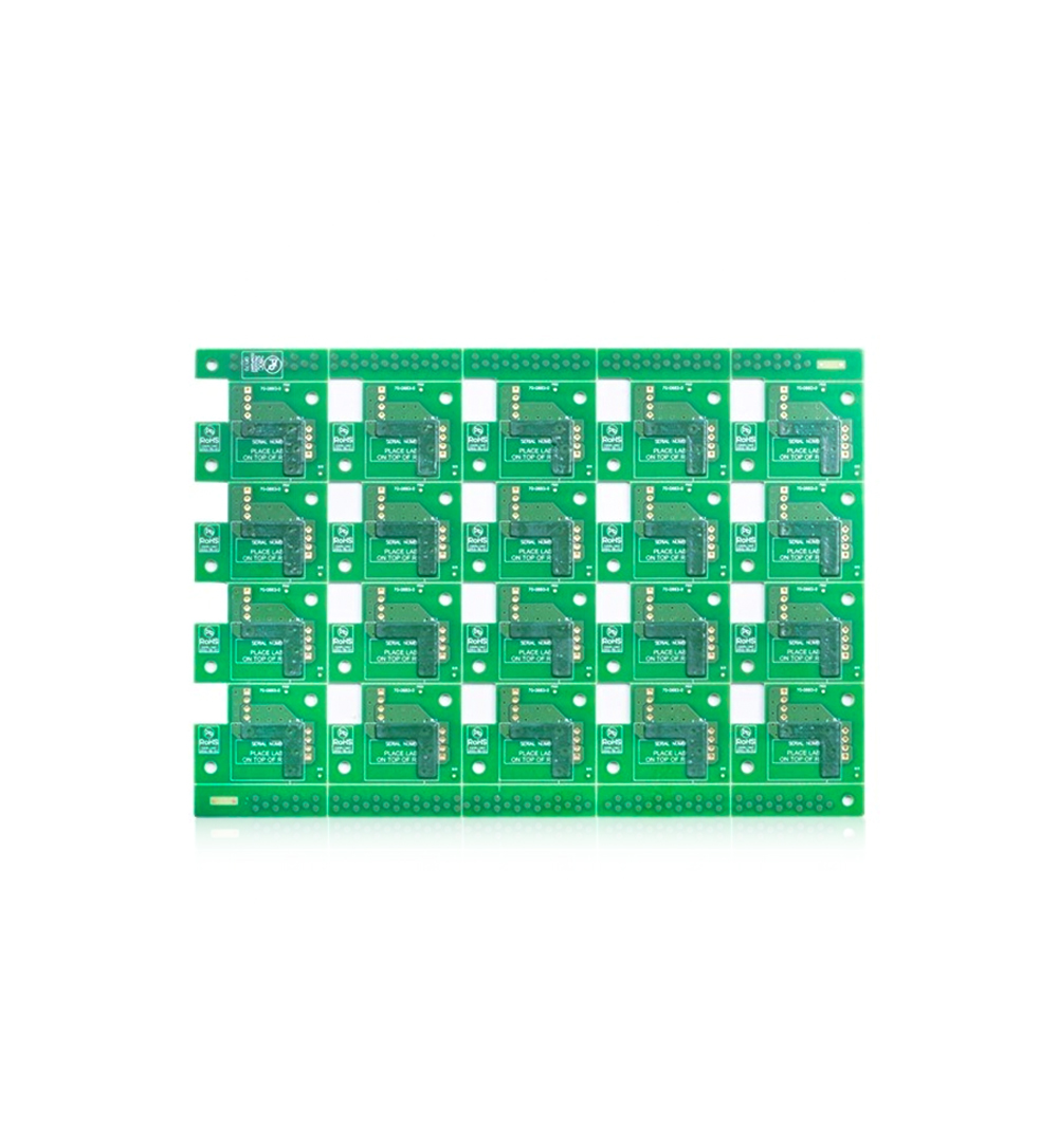
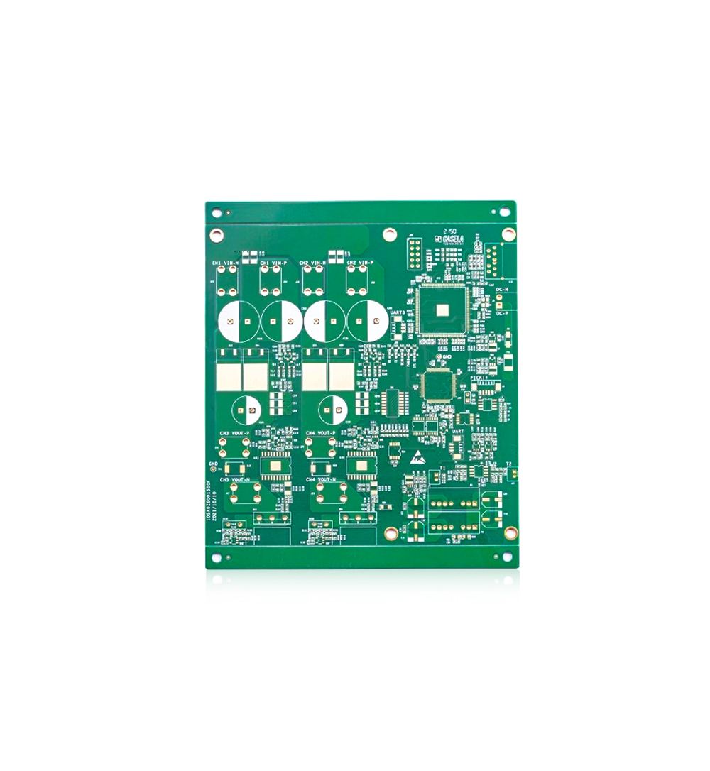
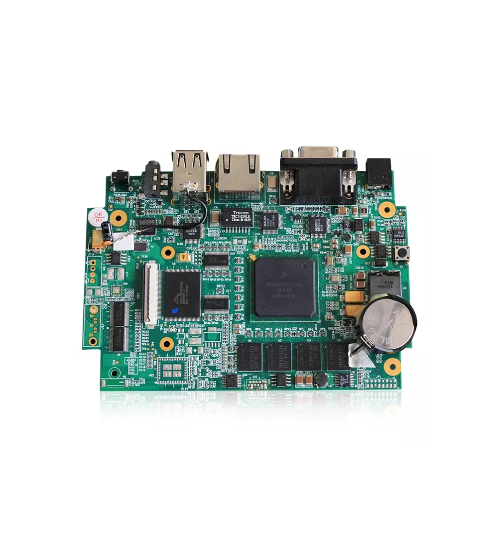
source:News release time:2023-03-24 Hits: Popular:PCB Assembly company

Because SMT generally uses infrared furnace thermal welding to achieve the welding of components, the layout of the component affects the quality of the solder joints and then affects the product rate of the product. For the PCB design of the radio frequency circuit, electromagnetic compatibility requires that each circuit module does not generate electromagnetic radiation as much as possible, and has a certain ability to anticromioled interference. Therefore, the layout of the component also directly affects the interference and anti -interference ability of the circuit itself. This is also directly related to the performance of the designed circuit. Therefore, in addition to considering the layout of ordinary PCB design when designing the PCB design of the RF circuit, it is necessary to consider how to reduce the interference between each part in the radio frequency circuit, how to reduce the interference of other circuits, and the circuit itself itself. Anti -interference ability. According to experience, the quality of the radio frequency circuit depends not only on the performance indicators of the radio frequency circuit board itself, but also a large part of it depends on the interaction between processing between the CPU processing board. Therefore, the reasonable layout is particularly important during PCB design.
General principle of layout: The components should be arranged at the same direction as much as possible. The phenomenon of reducing or even avoiding poor welding by choosing PCB into the melt system; at least 0.5mm between experience components can meet the melting tin of the meta device to meet the melting tin of the meta device. It is required that if the space of the PCB board is allowed, the spacing of the component should be as wide as possible. For double panels, one side should be designed as SMD and SMC components, and the other side should be separated components.
Pay attention to the layout:
*First determine the location of the interface components of other PCB boards or systems on the PCB board. We must pay attention to the cooperation between the interface components (such as the direction of the component, etc.).
*Because the volume of the palm supplies is very small, and the components are arranged tightly, the larger components must be given priority to determine the corresponding position, and consider the cooperation problem with each other.
*Carefully analyze the circuit structure, and perform segmentation of the circuit (such as high -frequency large circuits, mixing circuits, and demodulation circuits, etc.). The circuit that completes the same function should be arranged within a certain range to reduce the area of the signal loop; the filter network of each part of the circuit must be connected nearby, which can not only reduce the radiation, but also reduce the probability of being disturbed. According to the circuit, according to the circuit Anti -interference ability.
*Different the sensitivity of electromagnetic compatibility in the use of the unit circuit is different. When the components that are susceptible to interference in the circuit, the component of the part of the circuit should also avoid the interference source (such as the interference from the CPU from the data processing board, etc.).
Read recommendations:
Resin Plugged Hole Multilayer Circuit Board ENIG Surface 4L Halogen Free 1.6mm
Environmentally Friendly Aluminum PCB Board 1.6mm Single Layer
Welcome information, we will answer for you quickly

 No. 1 Jingtian Road, Xinsheng community, Longgang District, Shenzhen, Guangdong, China
 +86 13715096176
 Whatsapp/WeChat : +86 13715096176
 Kevin.kuang@xzgcircuits.com


 Return