source:Other information release time:2023-04-24 Hits: Popular:PCB Assembly company

1. Determine the number of layers of PCB
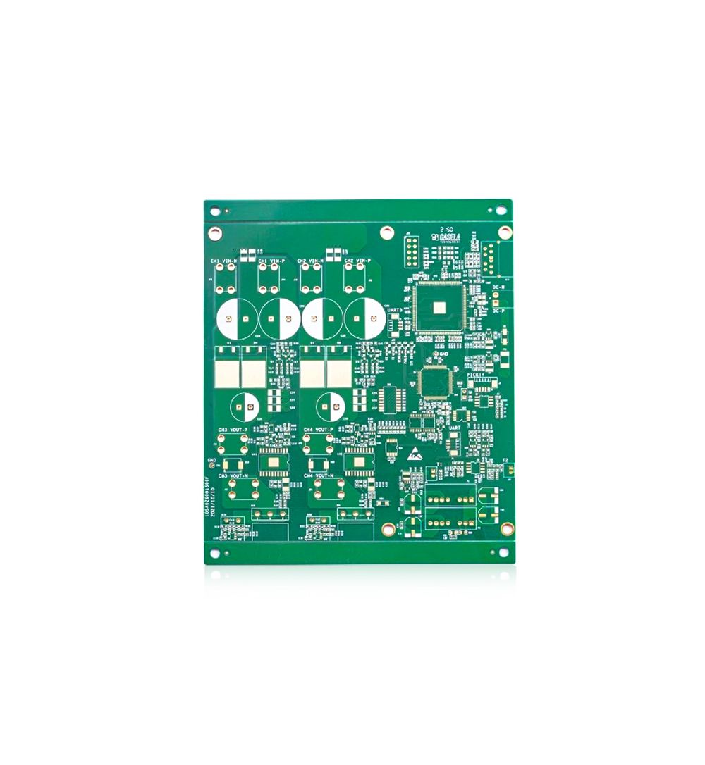
The size of the circuit board and the number of wiring layers need to be determined in the early stages of design. If the design requires the use of high-density ball grid array (BGA) components, the minimum number of wiring layers required for the wiring of these devices must be considered. The number of wiring layers and the stacking method directly affect the wiring and impedance of printed wires. The size of the board helps to determine the stacking method and printed wire width, achieving the desired design effect.
For many years, people have always believed that the fewer layers a circuit board has, the lower its cost. However, there are many other factors that affect the manufacturing cost of a circuit board. In recent years, the cost difference between multi-layer boards has greatly reduced. It is best to use more circuit layers at the beginning of the design and distribute the copper evenly to avoid discovering a small amount of signals that do not meet the defined rules and spatial requirements near the end of the design, forcing the addition of new layers. Careful planning before design will reduce a lot of trouble in wiring.
2. Design rules and limitations
The automatic routing tool itself does not know what to do. To complete wiring tasks, wiring tools need to work under the correct rules and limitations. Different signal lines have different wiring requirements, and all signal lines with special requirements need to be classified. Different design classifications are also different. Each signal class should have a priority, and the higher the priority, the stricter the rules. The rules involve printed wire width, maximum number of vias, parallelism, mutual influence between signal wires, and layer limitations, which have a significant impact on the performance of wiring tools. Careful consideration of design requirements is an important step in successful wiring.
3. Layout of components
To optimize the assembly process, DFM rules impose limitations on component layout. If the assembly department allows component movement, the circuit can be appropriately optimized for easier automatic wiring. The defined rules and constraints will affect layout design.
When laying out, it is necessary to consider the routing channel and through-hole area, as shown in Figure 1. These paths and areas are obvious to designers, but automatic wiring tools only consider one signal at a time. By setting wiring constraints and layers of signal wires that can be laid out, the wiring tool can complete the wiring as envisioned by the designer.
Read recommendations:
PI FR4 Double Layer Flex PCB Board Immersion Gold 2L Lightweight
FR4 1.6mm Double Sided Prototype PCB Board Immersion Gold 4mil
Welcome information, we will answer for you quickly

 No. 1 Jingtian Road, Xinsheng community, Longgang District, Shenzhen, Guangdong, China
 +86 13715096176
 Whatsapp/WeChat : +86 13715096176
 Kevin.kuang@xzgcircuits.com


 Return