source:Other information release time:2023-08-12 Hits: Popular:PCB Assembly company

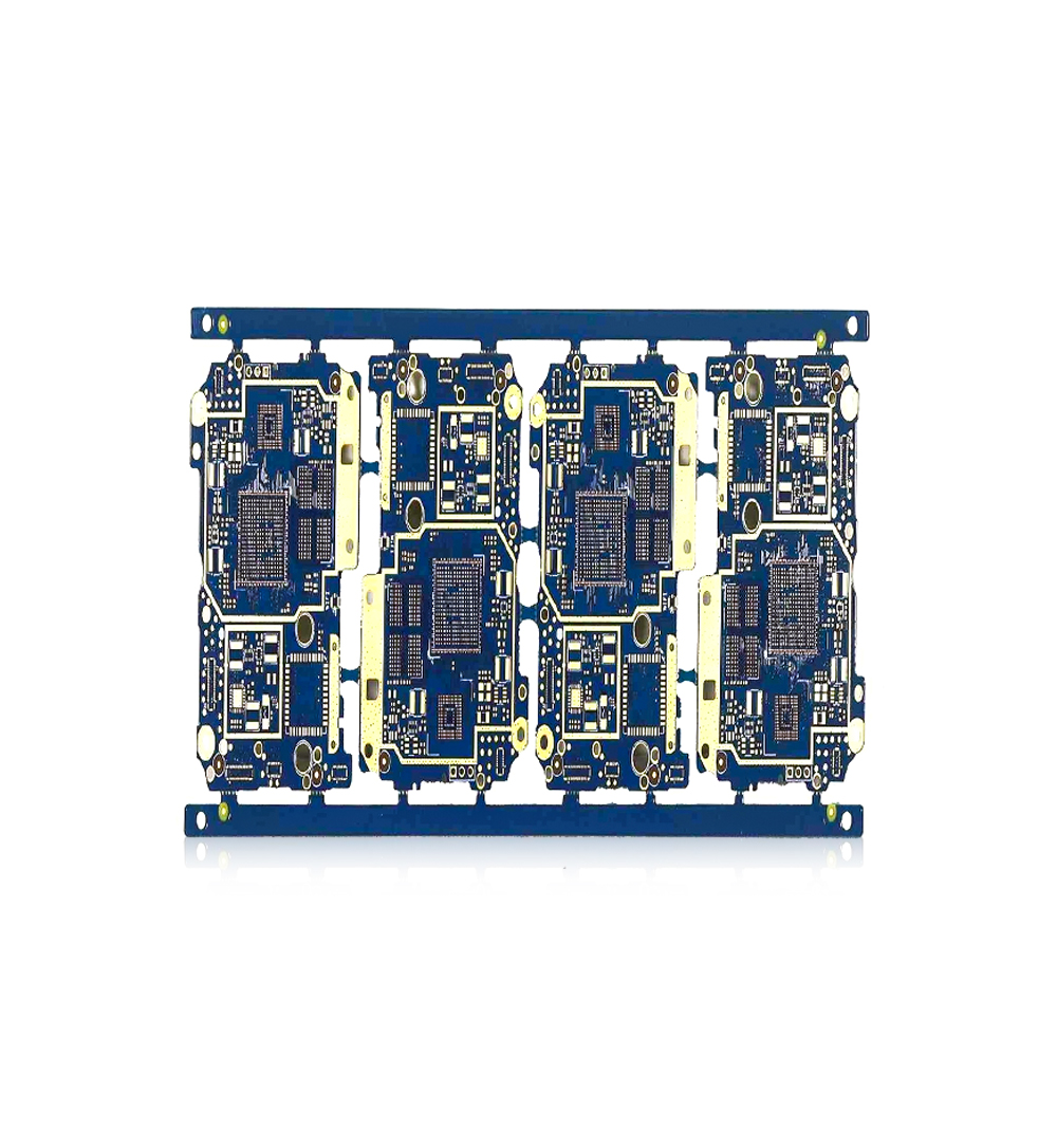
Determination of board shape, size, and number of layers
Any printed board has the problem of assembly with other structural components, so the appearance and size of the printed board must be based on the overall structure of the product. However, from the perspective of production technology, it should be as simple as possible. Generally, it is a rectangle with a Aspect ratio that is not too different, so as to facilitate assembly, improve production efficiency and reduce Labor burden.
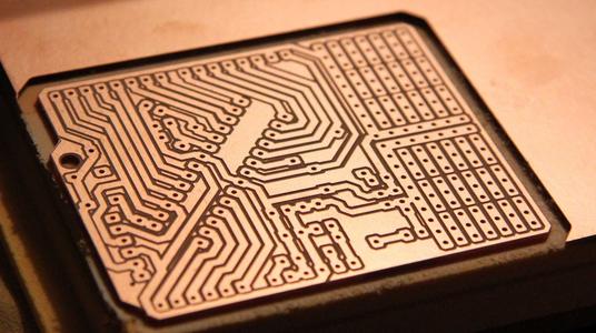
In terms of the number of layers, it must be determined based on the requirements of circuit performance, board size, and the density of the circuit. For multi-layer printed boards, four layer boards and six layer boards are the most widely used. For example, four layer boards include two wire layers (component surface and welding surface), one power layer, and one layer.
The layers of the multi-layer board should be symmetrical and preferably even numbered copper layers, such as four, six, eight layers, etc. Due to asymmetric lamination, the board surface is prone to warping, especially for surface mounted multilayer boards, which should be given more attention.
2. Location and placement direction of components
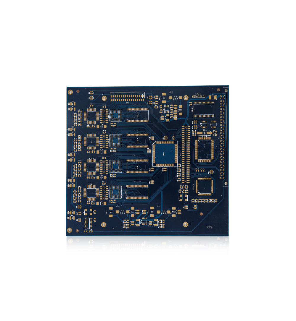
The position and placement direction of components should first be considered from the perspective of circuit principles to cater to the direction of the circuit. The rationality of placement will directly affect the performance of the printed circuit board, especially for high-frequency analog circuits, which have stricter requirements for the position and placement of devices. Reasonable placement of components, in a sense, has already indicated the success of the printed circuit board design. Therefore, when embarking on the layout of the printed circuit board and determining the overall layout, a detailed analysis of the circuit principle should be conducted. The location of special components (such as large-scale ICs, high-power transistors, signal sources, etc.) should be determined first, and then other components should be arranged to avoid possible interference factors as much as possible.
On the other hand, the overall structure of the printed circuit board should be considered to avoid uneven and disorderly arrangement of components. This not only affects the aesthetics of printed boards, but also brings a lot of inconvenience to assembly and maintenance work.
3. Requirements for wire layout and wiring area
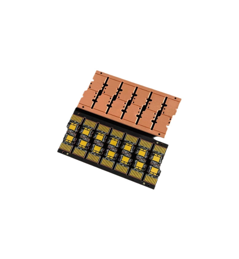
In general, multi-layer printed circuit board wiring is carried out according to the circuit function. When wiring in the outer layer, it is required to have more wiring on the welding surface and less wiring on the component surface, which is conducive to the maintenance and troubleshooting of the printed circuit board. Thin, dense wires and easily disturbed signal wires are usually arranged in the inner layer. A large area of copper foil should be evenly distributed between the inner and outer layers, which will help reduce the warpage of the board and also achieve a more uniform coating on the surface during electroplating. To prevent damage to printed wires and interlayer short circuits during machining, the distance between the conductive patterns in the inner and outer wiring areas and the board edge should be greater than 50mil.
Read recommendations:
1.6mm FR4 Double Sided Circuit Board Green Solder Mask For Medical Device
Welcome information, we will answer for you quickly

 No. 1 Jingtian Road, Xinsheng community, Longgang District, Shenzhen, Guangdong, China
 +86 13715096176
 Whatsapp/WeChat : +86 13715096176
 Kevin.kuang@xzgcircuits.com


 Return