source:Other information release time:2023-07-27 Hits: Popular:PCB Assembly company

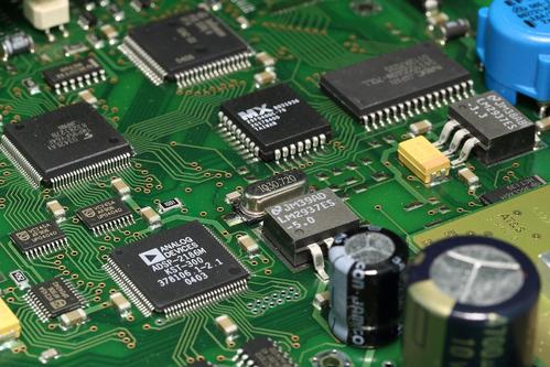
If only functional testing is used as a pass/fail screening without measuring calibration points, this section can be skipped as the application may not require the use of probes. In most cases, functional testing performs pass/fail detection because functional testing is very slow in diagnosing faults, especially when multiple faults occur. However, in some industries, functional testing is deepening into manufacturing processes, such as cellular phone manufacturing. Some manufacturers need to perform certain key measurements at the PCB level, that is, during the assembly process before final assembly, which is determined by the nature of mobile phones being easily phased out. In other words, mobile phones are designed to be assembled at a lower cost and are not easy to disassemble. Therefore, verifying their functionality before final testing can save on rework costs and reduce potential waste (as the phone can be damaged when disassembled).Solar Energy System
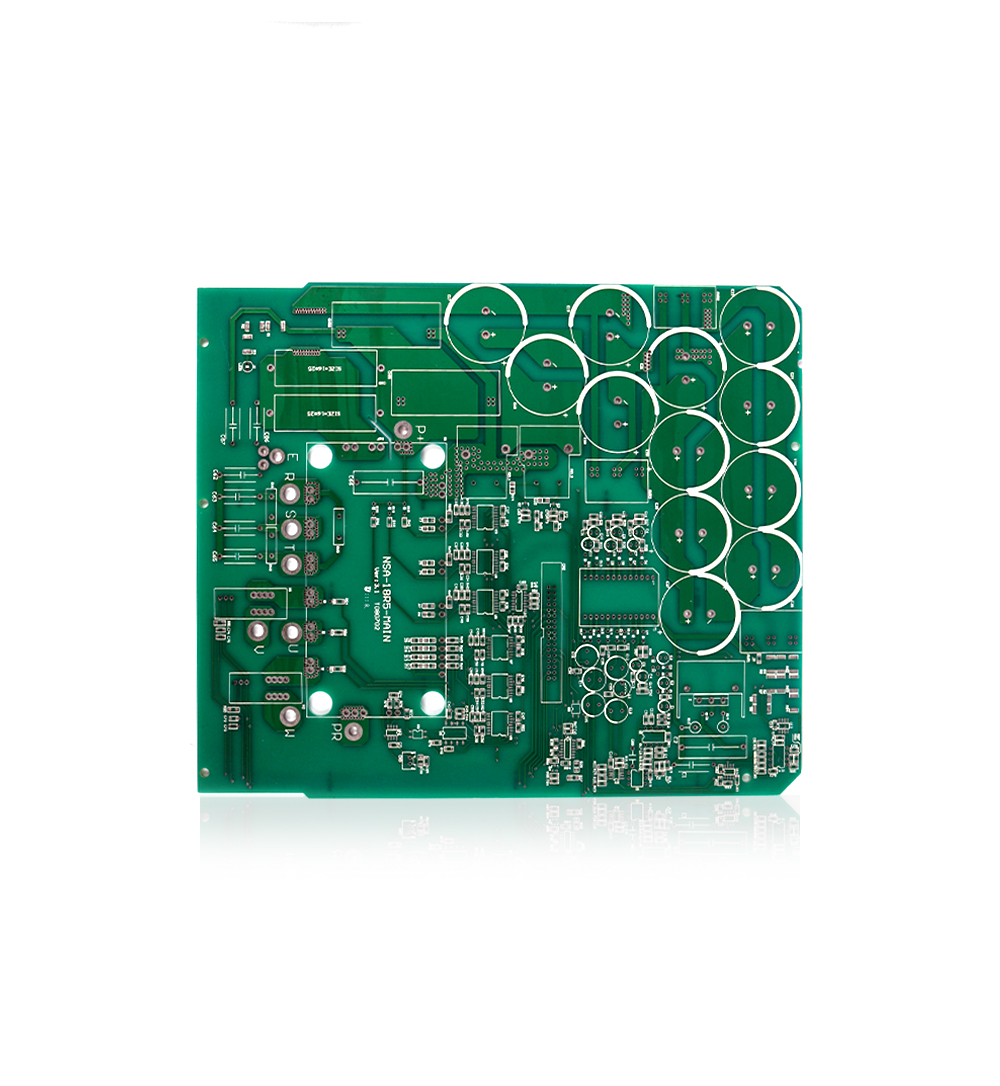
Therefore, enough Test point are required to probe PCB. For example, it is not convenient to check the J-shaped lead of a surface mounted device with a spacing of 20 mil, and BGA is even less possible. According to the recommendations of the American Surface-mount technology Association (SMTA), the minimum spacing between Test point is 0.040 inches. The spacing between pads depends on the element height, probe size, etc. around the test area, but 0.200 inch spacing should be the minimum requirement, especially for the manual detection area. Obviously, test fixtures and robotic probes are more precise.
Read recommendations:
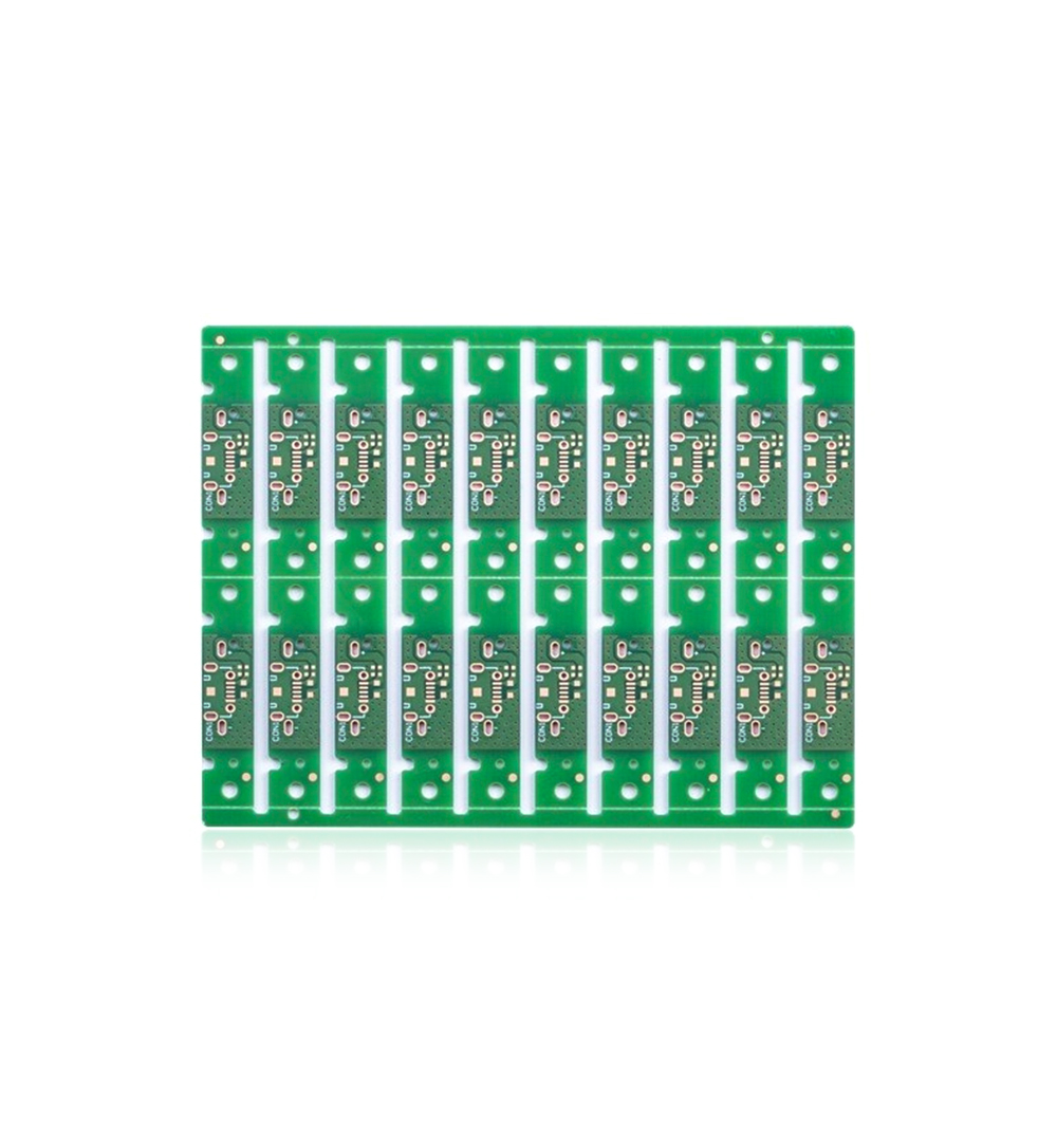
Multilayer Printed Circuit Board
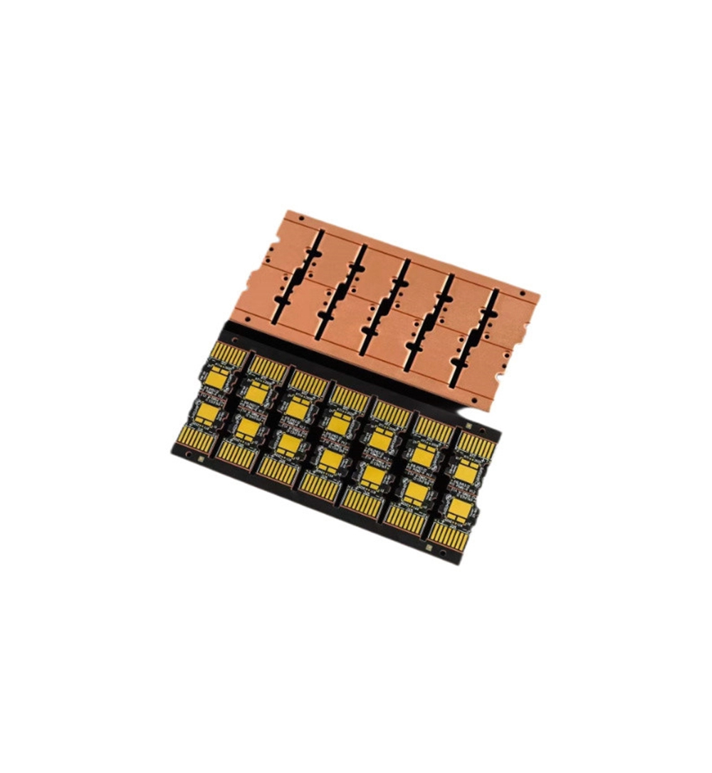
3mil 4L Rigid Flex PCB Black Solder Mask Diy Flexible Circuit Board
Welcome information, we will answer for you quickly

 No. 1 Jingtian Road, Xinsheng community, Longgang District, Shenzhen, Guangdong, China
 +86 13715096176
 Whatsapp/WeChat : +86 13715096176
 Kevin.kuang@xzgcircuits.com


 Return