source:News release time:2023-09-20 Hits: Popular:PCB Assembly company
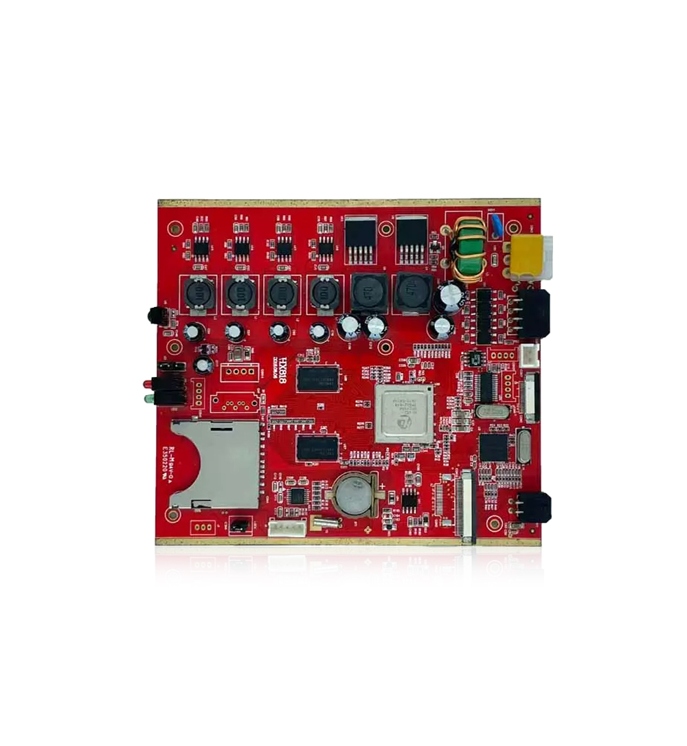
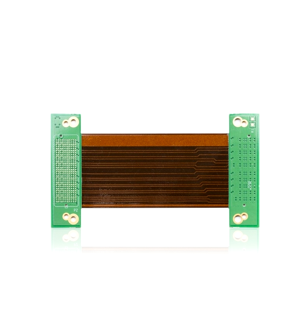
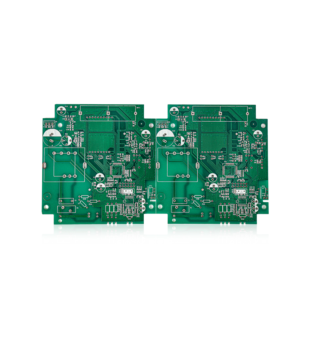
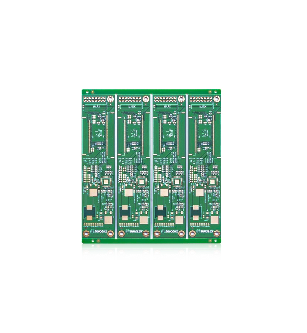
PCB multi layer boards are more complex in both design and manufacturing compared to single and double layer boards. So, what are the difficulties to pay attention to in PCB multi layer board sampling? Next, let the editor provide you with a detailed explanation.
1. Difficulties in interlayer alignment
Due to the numerous layers in multi-layer circuit boards, users have increasingly high requirements for PCB layer calibration. Considering the large unit size of multi-layer circuit boards, high temperature and humidity in the workshop environment, dislocation overlap caused by different core boards, and interlayer positioning methods, it is more difficult to control the alignment of multi-layer circuit boards.
2. Difficulties in making internal circuits
Multilayer circuit boards use special materials such as high TG, high-speed, high-frequency, thick copper, and thin dielectric layers, which put forward high requirements for internal circuit production and graphic size control. Small width and line spacing, increased open circuit and short circuit, and low qualification rate; Multiple thin line signal layers increase the probability of AOI leakage detection in the inner layer; The inner core board is thin, prone to wrinkling, poor exposure, and prone to curling during etching.
3. Difficulties in compression manufacturing
Many inner core boards and semi cured boards are superimposed, and defects such as sliding plates, delamination, resin voids, and residual bubbles are prone to occur in stamping production. In the design of laminated structures, full consideration should be given to the heat resistance, voltage resistance, adhesive content, and dielectric thickness of the materials, and a reasonable material pressing plan for multi-layer circuit boards should be formulated.
4. Difficulties in drilling production
The use of high TG, high-speed, high-frequency, thick copper special plates increases the difficulty of drilling roughness, drilling burrs, and removing drilling stains.
Read recommendations:
Halogen Free FR4 Multilayer Printed Circuit Board 1.6mm 10mil Impedance Control
Welcome information, we will answer for you quickly

 No. 1 Jingtian Road, Xinsheng community, Longgang District, Shenzhen, Guangdong, China
 +86 13715096176
 Whatsapp/WeChat : +86 13715096176
 Kevin.kuang@xzgcircuits.com


 Return