source:Other information release time:2022-12-01 Hits: Popular:PCB Assembly company

The following principles shall be observed when determining the location of special electronic components:
1. The position occupied by the positioning hole and fixing bracket of the printed board shall be reserved.
2. Shorten the connection between high-frequency components as much as possible, and try to reduce their distribution parameters and mutual electromagnetic interference. Components susceptible to interference shall not be too close to each other, and input and output components shall be as far away as possible.
3. There may be high potential difference between some components or wires. The distance between them should be increased to avoid accidental short circuit caused by discharge. Components with high voltage shall be arranged at places where it is not easy to reach during commissioning.
4. Components weighing more than 15g shall be fixed with brackets and then welded. Those large, heavy and heat generating components should not be installed on the printed board, but should be installed on the chassis bottom of the whole machine, and heat dissipation should be considered. The thermal element shall be far away from the heating element.
5. For the layout of adjustable components such as potentiometers, adjustable inductance coils, variable capacitors, microswitches, etc., the structural requirements of the whole machine shall be considered. If it is adjusted in the machine, it should be placed on the printed board where it is convenient for adjustment; If it is adjusted outside the machine, its position shall be consistent with the position of the adjustment knob on the chassis panel.
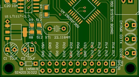
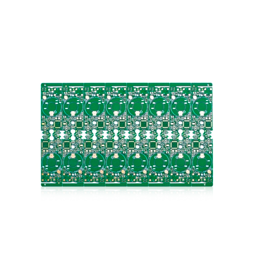
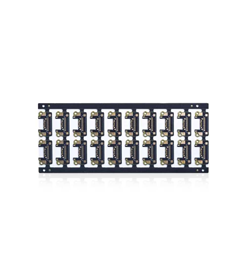
The layout of pcb multilayer circuit board for electronic components of the circuit shall meet the requirements of anti-interference design:
1. Arrange the position of each functional circuit unit according to the circuit flow, so that the layout is convenient for signal flow and the signal is kept in the same direction as far as possible.
2. For circuits operating at high frequencies, the distribution parameters between components should be considered. For general circuits, components shall be arranged in parallel as far as possible. In this way, it is not only beautiful, but also easy to assemble and weld, and easy to mass produce.
3. Take the core components of each functional circuit as the center, and arrange around it. Components shall be uniformly, neatly and compactly arranged on the pcb multilayer circuit board. Try to reduce and shorten the lead wires and connections between components.
4. The electronic components located at the edge of the circuit board are generally not less than 2mm away from the edge of the circuit board. The optimal shape of the circuit board is rectangle. The length and width are 3:2 or 4:3. The size of the circuit board is greater than 200 × For 150mm, the mechanical strength of the circuit board shall be considered.
Read recommendations:
Welcome information, we will answer for you quickly

 No. 1 Jingtian Road, Xinsheng community, Longgang District, Shenzhen, Guangdong, China
 +86 13715096176
 Whatsapp/WeChat : +86 13715096176
 Kevin.kuang@xzgcircuits.com


 Return