source:News release time:2023-03-03 Hits: Popular:PCB Assembly company

The design is designed according to the requirements of the pads to achieve a small diameter. This diameter is 0.5mm larger than the large diameter of the small pores of the welding terminal. It must provide test pads for all nodes according to the requirements of ANSI/IPC 2221. Electrical connection points between multiple components. One test pad requires a signal name (node signal name), X-Y coordinate shaft related to the benchmark point of printed circuit board, and the coordinate position of the test pad (indicates that the test pad Which side of the printing circuit board). You need to provide information for SMT with a fixed device, and you also need to print the temperature compliance technology of the circuit board installation and layout, so as to "in the circuit test fixed device" or it is usually called the "nail bed fixed fixed fixation of the nail bed fixed. With the help of "device", it promotes testability in the circuit. To achieve this, it needs:
1) The diameter of the test pads specially used for detection should not be less than 0.9mm.
2) Test the space around the pads should be greater than 0.6mm and less than 5mm. If the height of the component is greater than 6.7mm, the test pad should be placed outside the component 5mm.
3) Do not place any meta device or test pad within 3mm from the edge of the circuit board.
4) Test pads should be placed in the center of 2.5mm holes in a grid. If possible, the standard probe and a more reliable fixed device are allowed.
5) Do not rely on the edge of the connector to perform pad test. Test probes can easily damage gold -plated pointers.
6) Avoid detection on both sides of the printing-printed circuit board. Put the test on the non -component/welding surface of the printed circuit board.
Read recommendations:
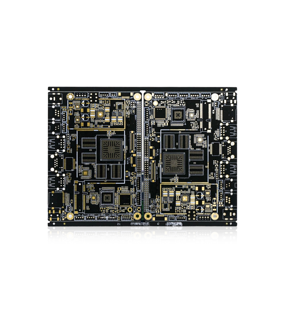
Multilayer Printed Circuit Board
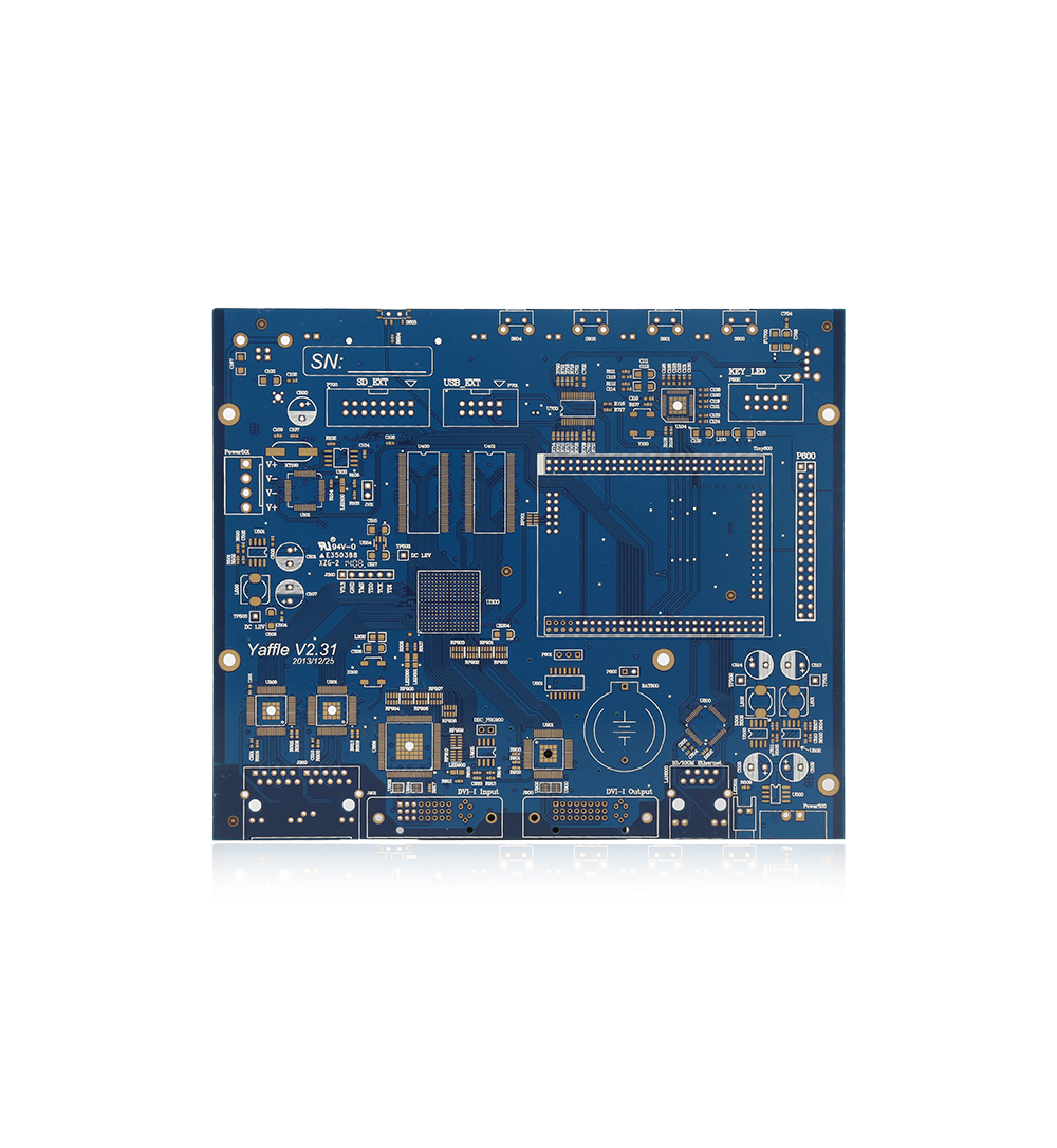
FR4 1.6mm Double Sided Prototype PCB Board Immersion Gold 4mil
Welcome information, we will answer for you quickly

 No. 1 Jingtian Road, Xinsheng community, Longgang District, Shenzhen, Guangdong, China
 +86 13715096176
 Whatsapp/WeChat : +86 13715096176
 Kevin.kuang@xzgcircuits.com


 Return