source:Other information release time:2023-02-14 Hits: Popular:PCB Assembly company

Electromagnetic compatibility refers to the ability to work and effectively work in various electromagnetic environments in various electromagnetic environments. The purpose of electromagnetic compatibility design is to enable electronic devices to inhibit all kinds of foreign interference, enable electronic devices to work normally in a specific electromagnetic environment, and at the same time reduce electromagnetic interference of electronic equipment itself.
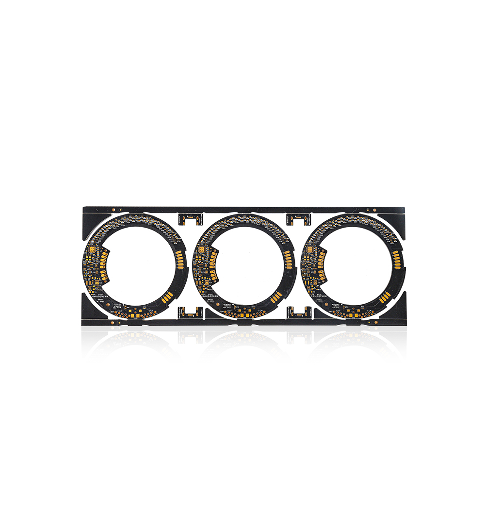
Choosing a reasonable wire width due to the impact interference caused by the transient current on the printing lines is mainly caused by the inductor component of the printed wire, so you should minimize the inductance of the printed wire. The inductance of the printed wire is proportional to its length, and it is inversely proportional to its width. Therefore, short and refined wires are beneficial to inhibit interference. The signal line of clock leads, row drives or bus drives often contains large transient current, and the printed wires should be as short as possible. For separate component circuits, when the width of the printed wire is about 1.5mm, it can fully meet the requirements; for integrated circuits, the width of the printed wire can be selected between 0.2 and 1.0mm.
Using the correct wiring strategy to use equal wiring can reduce the wire inductance, but the interdependence and distributed capacitors between the wires increase. If the layout allows, it is better to use the well -shaped mesh wiring structure. The specific method is the horizontal wiring of the printing board. The other side is vertically wiring, and then connected with a metal hole at the crosshole.
In order to curb the string between the wire wire wires, you should avoid long -distance equal wiring as much as possible when designing the wiring, and pull the distance between the wires and the line as much as possible. Setting a ground printing line between some signal lines that are very sensitive to interference can effectively suppress the string disturbances. In order to avoid electromagnetic radiation when high -frequency signals are generated when printed through the wires,
Read recommendations:
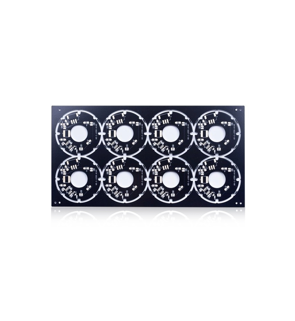
Metal Core 0.8mm Led Street Light Pcb Aluminium Pcb Board For Led
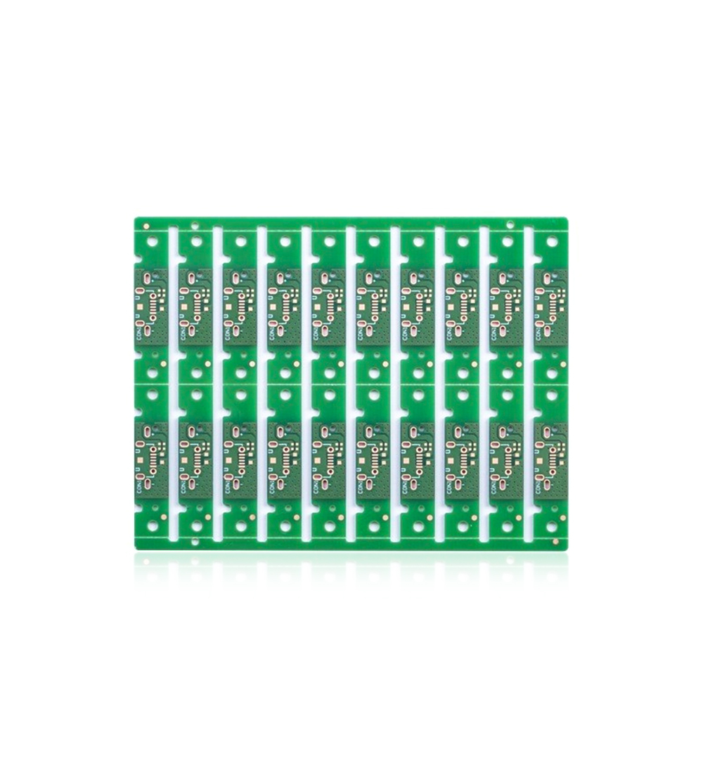
Blue Solder Mask Double Sided PCB Board High TG TG170 S1000-2
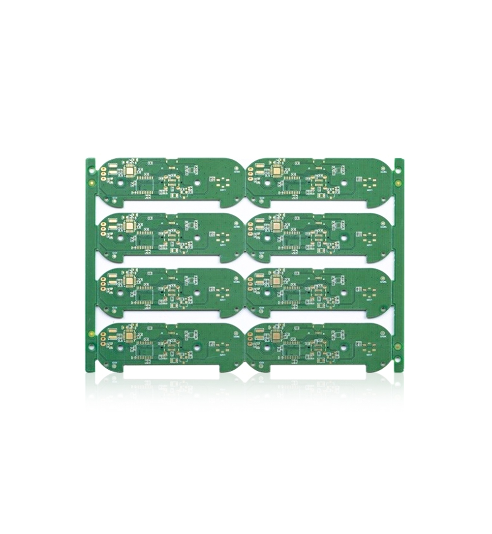
0.8mm Single Layer Rigid Flex PCB Quick Turn 0.5oz Laser Prototyping
Welcome information, we will answer for you quickly

 No. 1 Jingtian Road, Xinsheng community, Longgang District, Shenzhen, Guangdong, China
 +86 13715096176
 Whatsapp/WeChat : +86 13715096176
 Kevin.kuang@xzgcircuits.com


 Return