source:Other information release time:2023-03-10 Hits: Popular:PCB Assembly company

1: Selection of the width of the printing wire:
The small width of the printing wire is related to the current flow of the flowing wire:
The wire width is too small, and the transliteration of the wires is large, and the voltage on the line is also large, which affects the performance of the circuit.
The width is too wide, the wiring density is not high, and the area of the board increases. In addition to increasing costs, it is not conducive to miniaturization.
Therefore, the line width of 1--2.54mm (40--100mil) can meet the general application requirements. The ground wire and power supply on the high-power device board can appropriately increase the wire width according to the power size, and the small power number can be appropriately increased. On the circuit, in order to increase the wiring density, the small wire width can be satisfied by 0.254--1.27mm (10--15mil) to meet.
In the same circuit board, the power line. The ground line is thicker than the signal line.
2: Line spacing: When it is 1.5mm (about 60mil), the insulation resistance of the lines between the lines is greater than 20m Euros, and the resistance voltage of the line can reach 300V. When the line spacing is 1mm (40mil), the inter -line resistance voltage is 200V. Therefore On the circuit board with low voltage (between line voltage is not greater than 200V), the wire spacing is 1.0--1.5mm (40--60mil) at a low voltage circuit, such as the digital circuit system, there is no need to consider the breakdown voltage, as long as the production process is required Allow, it can be very small.
3: pad: For the resistance of 1/8W, the diameter of the pads is 28mil.
For 1/2W, the diameter is 32mil, the lead hole is too large, and the width of the copper ring of the pads is relatively reduced, resulting in the decrease in the adhesion of the pad. It is easy to fall off, the lead hole is too small, and the component is difficult to install.
4: Draw the roadside frame:
The short distance between the border and the component pin pad should not be less than 2mm, (generally more reasonable to take 5mm), otherwise it will be difficult.
Read recommendations:
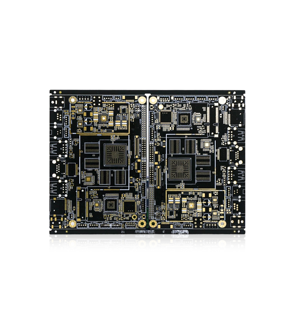
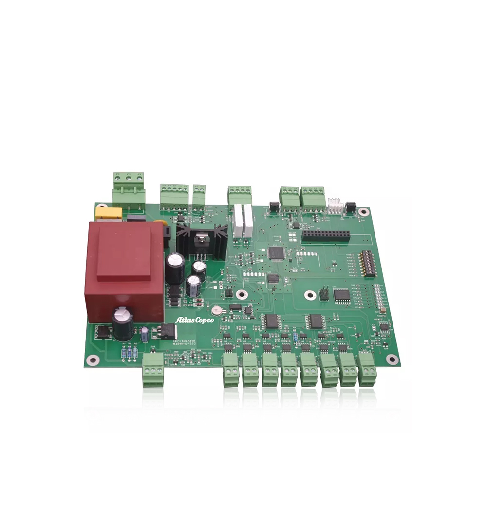
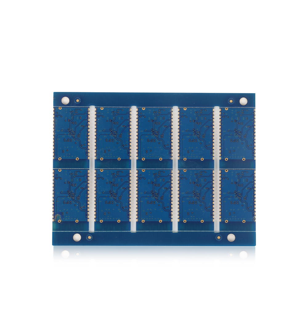
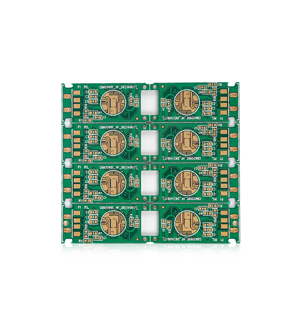
Halogen Free FR4 Double Sided PCB 5mil Immersion Gold 1.6mm
6L 2OZ Multilayer Printed Circuit Board FR4 TG135 Multi Layer Pcb Green Solder Mask
HASL FR4 Single Sided Copper PCB Board White Solder Mask 35um Thickness
Welcome information, we will answer for you quickly

 No. 1 Jingtian Road, Xinsheng community, Longgang District, Shenzhen, Guangdong, China
 +86 13715096176
 Whatsapp/WeChat : +86 13715096176
 Kevin.kuang@xzgcircuits.com


 Return