source:Other information release time:2023-07-24 Hits: Popular:PCB Assembly company

Additive method is now commonly used on a pre coated thin copper substrate, covered with photoresist (D/F), exposed to ultraviolet light and developed to expose the desired area. Then, electroplating is used to thicken the formal copper thickness on the circuit board to the required specifications, and a layer of etching resistant agent - metal thin tin is coated. Finally, the photoresist is removed (this process is called stripping), and the copper foil layer under the photoresist is etched off.
The stacking method is one of the methods for making multi-layer printed circuit boards. The outer layer is wrapped after the inner layer is made, and then the outer layer is processed by subtraction or addition. Continuously repeating the action of the layering method can result in multiple layers of printed circuit boards, which is the sequential layering method.
Layering method
The layer adding method is one of the methods for making multi-layer printed circuit boards, as the name suggests, which involves adding layers of printed circuit boards one by one. Each additional layer is processed to the desired shape.
Read recommendations:
Halogen Free FR4 Double Sided PCB 5mil Immersion Gold 1.6mm
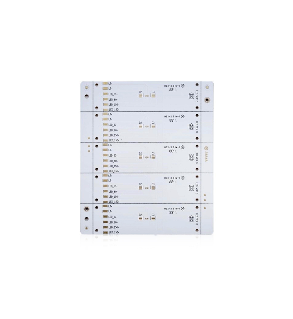
HASL FR4 Single Sided Copper PCB Board White Solder Mask 35um Thickness
Welcome information, we will answer for you quickly

 No. 1 Jingtian Road, Xinsheng community, Longgang District, Shenzhen, Guangdong, China
 +86 13715096176
 Whatsapp/WeChat : +86 13715096176
 Kevin.kuang@xzgcircuits.com


 Return