source:Other information release time:2023-10-22 Hits: Popular:PCB Assembly company

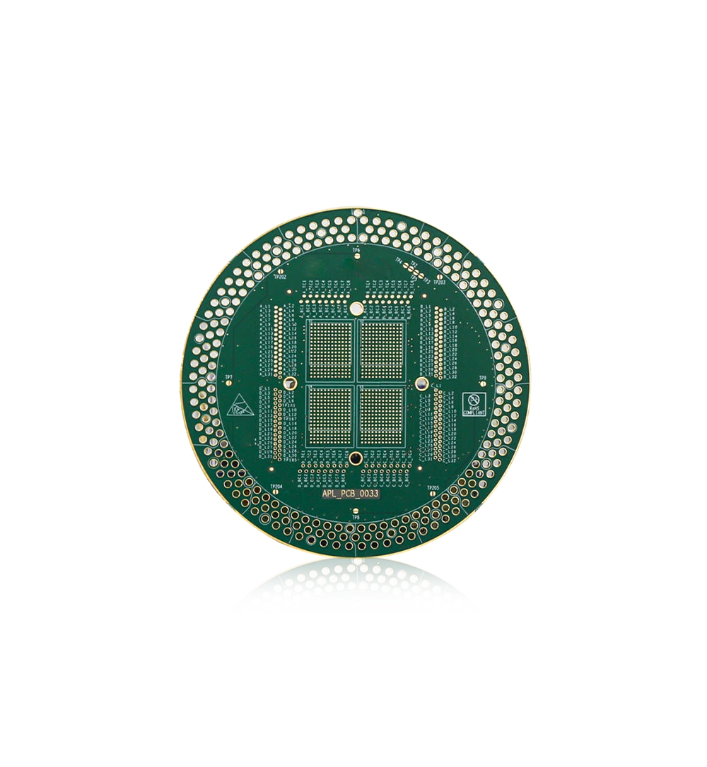
Looking at a complex PCB circuit board, such as a computer's motherboard, one may notice several tracks going nowhere and ending abruptly. However, closer inspection with a magnifying glass will reveal more detail at the point where the track ends. Most likely, you'll see that it ends with a small circuit board pad, not much larger than the width of the track itself, with a hole or no hole in its center. This is about the via technology of the circuit board factory.
In fact, the track does not terminate but continues to travel, albeit on a different layer, hidden beneath the outermost layer of the PCB. The ends of the pads are actually small tubes threaded through the insulating material that electrically connect the two parts of the track. In circuit board pattern maker terminology, this arrangement that allows the track to continue but on a different layer is called a circuit board via.Solar Energy System
Multilayer PCB circuit boards use different types of vias for various purposes. There may be through-hole vias, blind vias, and buried vias in the same circuit board. Although the construction of all vias is the same, their naming depends on the origin and termination layer. For example, a via that originates from the outermost layer, passes through the board, and terminates in another outermost layer is a via. On its way through the layers of the board, it may or may not be connected to intermediate layers, depending on the necessity of the circuit.
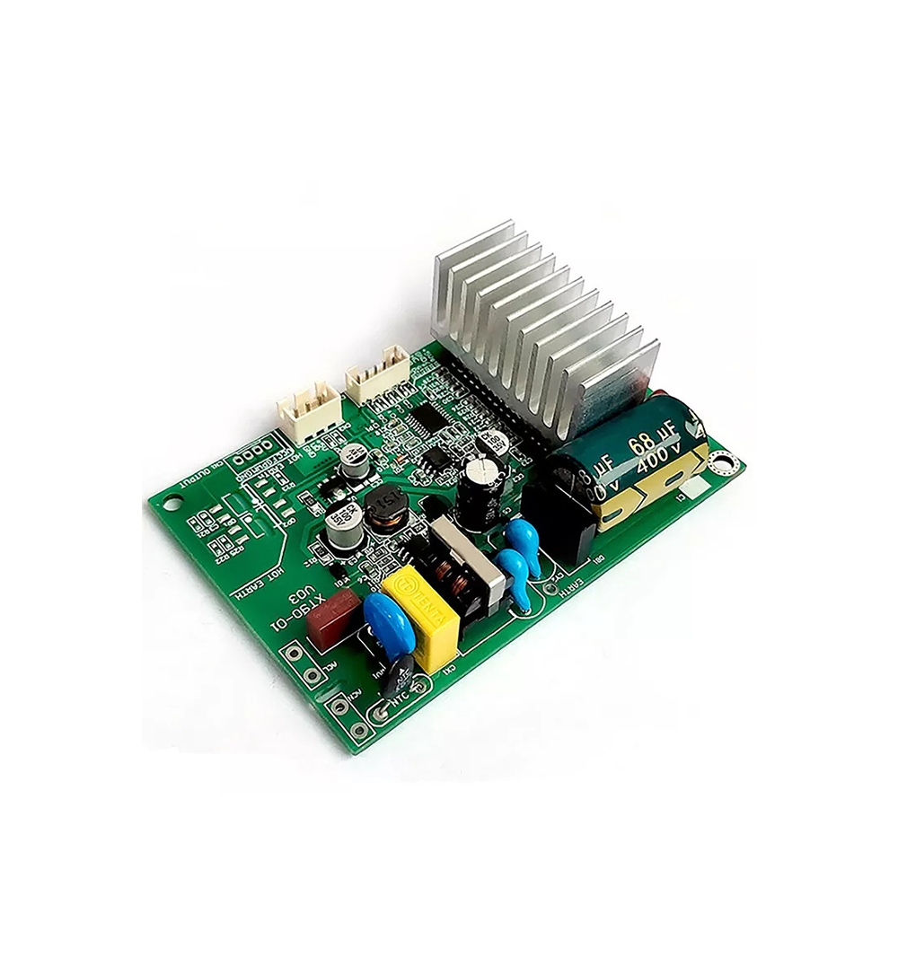
Printed circuit board/circuit board
Blind vias originate from one of the outermost layers but terminate in the middle layer, so are only visible on the starting layer. It may or may not be connected to other layers in between. The buried via is not visible from either of the outermost layers because it originates from one inner layer and terminates in another inner layer, possibly connecting other layers in between. By design, the via consists of two external pads and a copper tube that electrically connects them. Two external pads are located on the origin and termination layers of the PCB, while anti-pads on all intermediate layers allow the copper pipes to be electrically isolated from the circuitry on those layers as they pass through them.
Although the two external pads and the anti-pad are part of the layout pattern and etched onto the PCB, the electrodeposition process forms the copper tubes that connect the two. While through-holes may be found in regular PCB multilayer circuit boards, these are less likely in high-density interconnect or HDI circuit boards.
Read recommendations:
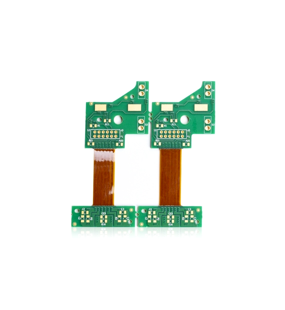
Polymer Film Flex PCB Board 0.1mm 2 Layer Rigid Flex Pcb Lightweight
Welcome information, we will answer for you quickly

 No. 1 Jingtian Road, Xinsheng community, Longgang District, Shenzhen, Guangdong, China
 +86 13715096176
 Whatsapp/WeChat : +86 13715096176
 Kevin.kuang@xzgcircuits.com


 Return