source:News release time:2023-02-09 Hits: Popular:PCB Assembly company

1. Engineering design:
Precautions should be made when the printing board design:
A. The arrangement of semi -solidarial tablets should be symmetrical. For example, the thickness between the six -layer PCB board, the thickness between the 1 to 2 and 5 to 6 layers should be the same as the number of semi -curing tablets, otherwise it will be easy to warp after the layer pressure.
B. Multi -layer circuit board core board and semi -solidarial chip should use products of the same supplier.
C. The line area of the outer layer A and B side should be as close as possible. If the A side is a large copper surface, and the B side only takes a few lines, this printed board is easy to warrate after etching. If the area of the two sides is too large, you can add some independent grids to the sparse side to balance.
2. Baked board before the feeding:
PCB thick copper plates (150 degrees Celsius, 8 ± 2 hours) the purpose is to remove the moisture in the board, and at the same time make the resin in the board completely solidify, and further eliminate the remaining stress in the board. helpful. At present, many double -sided and multi -layer PCB boards still insist on the steps before or after the feeding. However, there are also some plate factories. At present, the time regulations of the PCB plants are also inconsistent. From 4-10 hours, it is recommended to determine according to the grade of the printed board and the customer's requirements for warranty. After cutting into a panel, it is used to bake the whole piece of material. Both methods are feasible. It is recommended to cut the board after cutting. The inner plate should also be baked.
3. The latitude and weft of semi -curing tablets:
After the pressure of the semi -cured chin layer is pressured and weft, the contraction rate is different. Otherwise, it is easy to lead to the warpage after layer pressure, and it is difficult to correct it even if the pressure bakery is added. Many reasons for the warpage of the multi -layer plate are caused by the latitude and weft of semi -solidified chips during laminar pressure.
How to distinguish between Jingwei? The direction of the semi -curved film rolled up is the direction, and the width direction is the weft direction; for the copper foil board, the long side is weft, and the short side is the meridian.
Read recommendations:
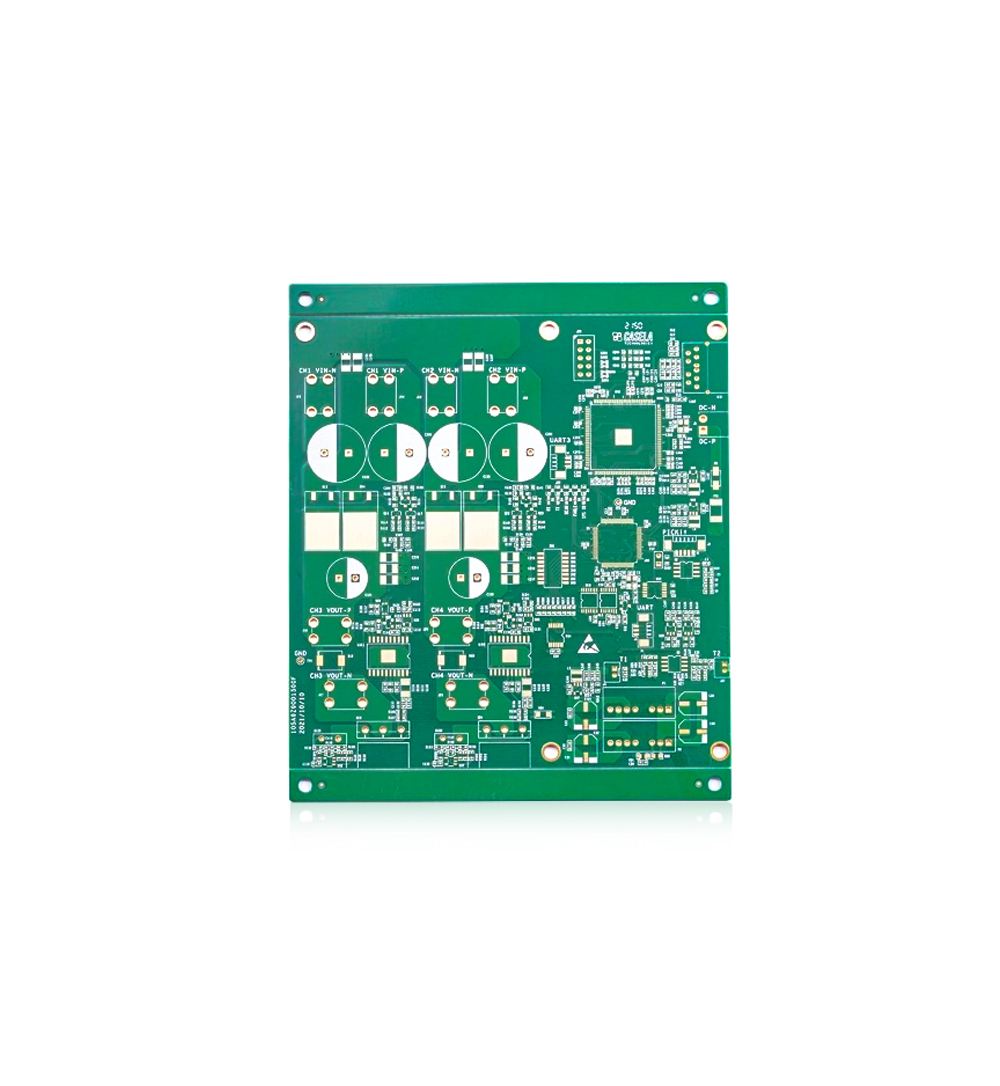
HASL FR4 Single Sided Copper PCB Board White Solder Mask 35um Thickness
1.5oz Multilayer Pcb Fabrication FR4 Printed Circuit Board Pcb 4 Layer
Welcome information, we will answer for you quickly

 No. 1 Jingtian Road, Xinsheng community, Longgang District, Shenzhen, Guangdong, China
 +86 13715096176
 Whatsapp/WeChat : +86 13715096176
 Kevin.kuang@xzgcircuits.com


 Return