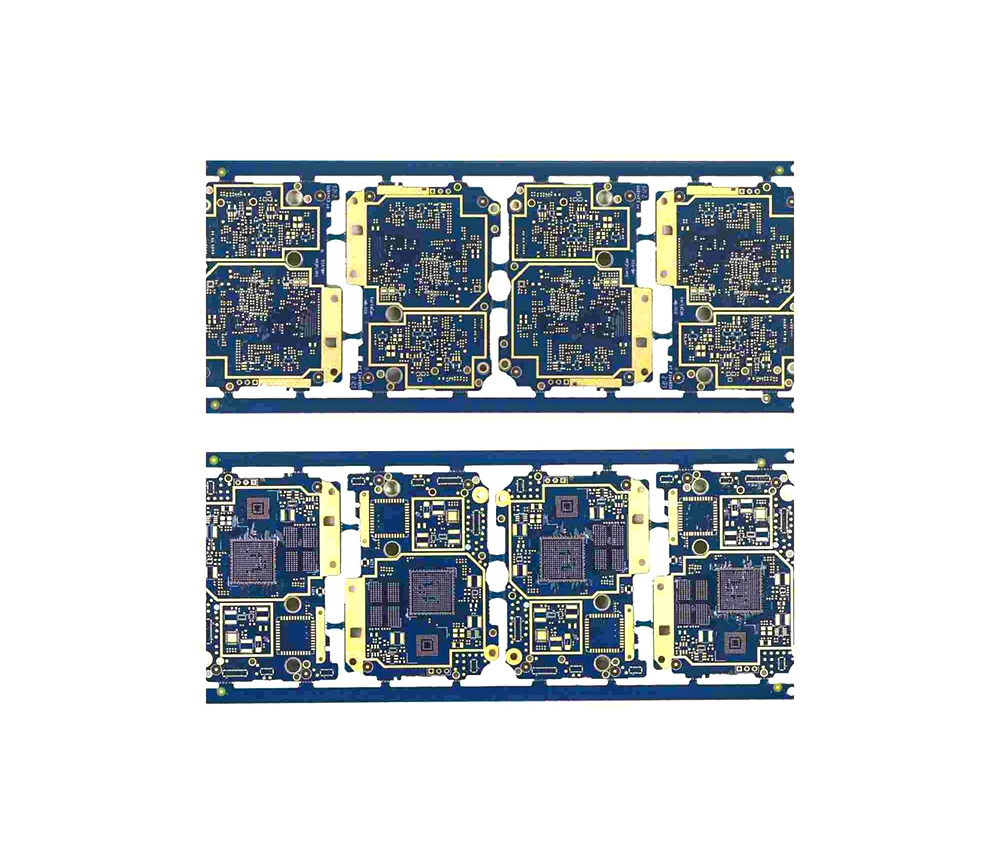
source:News release time:2022-11-08 Hits: Popular:PCB Assembly company

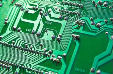
In short, the purpose of setting test points is to test whether the components on the circuit board meet the specifications and solderability. For example, to check whether the resistance on a circuit board is correct, the simplest way is to measure the two ends of the circuit board with a multimeter.
However, there is no way to use an electric meter to slowly measure the correctness of each resistance, capacitance, inductance, and even IC circuit on each board in a mass production circuit board factory. Therefore, the so-called ICT (In Circuit Test) automatic testing machine appears. It uses multiple probes (commonly called "Bed Of Nails" fixtures) to simultaneously contact all parts and circuits on the board that need to be measured, Then, the characteristics of these electronic parts are measured in sequence through program control, mainly in sequence, supplemented by juxtaposition. Generally, the test of all parts of a general board can be completed in about 1-2 minutes. Depending on the number of parts on the circuit board, the more parts, the longer the time.
However, if these probes directly contact the electronic parts or their solder legs on the circuit board, it is likely to crush some electronic parts, which is counterproductive. So smart engineers invented a "test point". An additional pair of round dots were introduced at both ends of the part. There is no mask on it, so the test probe can contact these dots, It does not need to directly contact the electronic parts being measured.
In the early days when the circuit board was still a traditional plug-in (DIP), PCB manufacturers did use the solder legs of parts as test points, because the solder legs of traditional parts were strong enough to be free from pin pricking. However, misjudgment of poor probe contact often occurred, because ordinary electronic parts were wave soldered or SMT soldered, A layer of residual film of solder paste flux is usually formed on the surface of its solder. The impedance of this film is very high, which often leads to poor contact of the probe. Therefore, it is often seen that the test operators of the PCB factory production line often blow hard with an air gun, or wipe these places that need to be tested with alcohol.
In fact, the probe may have poor contact at the test point after wave soldering. Later, after the prevalence of SMT, the situation of test misjudgment has been greatly improved, and the application of test points has also been given a great responsibility. Because SMT parts are usually fragile and cannot withstand the direct contact pressure of the test probe, the use of test points allows the probe to not directly contact the parts and their weld legs, which not only protects the parts from damage, but also indirectly greatly improves the reliability of the test, because there are fewer misjudgments.
Read recommendations:
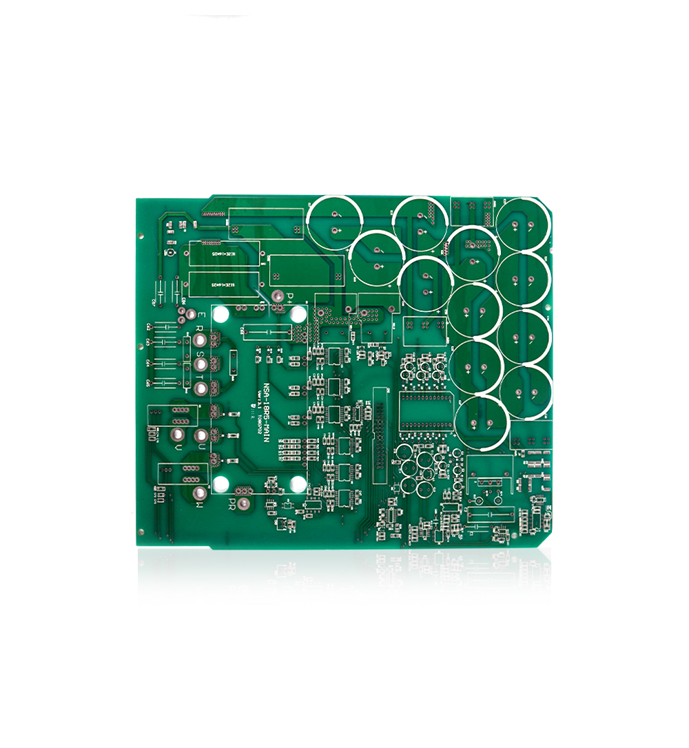
Environmentally Friendly Aluminum PCB Board 1.6mm Single Layer
Welcome information, we will answer for you quickly

 No. 1 Jingtian Road, Xinsheng community, Longgang District, Shenzhen, Guangdong, China
 +86 13715096176
 Whatsapp/WeChat : +86 13715096176
 Kevin.kuang@xzgcircuits.com


 Return