source:Other information release time:2023-02-06 Hits: Popular:PCB Assembly company

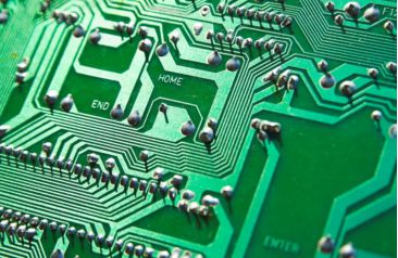
The products with the most HDI technology in the early days are mainly functional mobile phones and smart phones. Such products account for more than half of HDI high-density circuit boards, while Any-Layer HDI (any high density connecting board) is high as high as high The biggest difference between the order HDI production process is that the biggest difference between the general HDI circuit board is that most HDI is performed by the drilling process of the drilling process. Open each layer of connecting design.
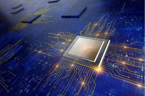
For example, the production method of Any-Layer HDI can generally reduce about 40 % of the PCB volume. At present, Any-Layer HDI has been used for Apple iPhone 4, or more novel smartphones, with higher density integration motherboards with higher density integration motherboards Reduce the thickness of the product design, so that the product design can ask the market in a lighter design pattern. However, Any-Layer HDI is made of laser blind hole. It is relatively difficult to process and produce by the line, and the cost is higher than that of the average circuit board. At present, only high-unit mobile devices are used.
Read recommendations:
1.6mm FR4 Double Sided Circuit Board Green Solder Mask For Medical Device
Multilayer Printed Circuit Board 1OZ 4 Layer Multilayer Pcb FR4 TG170 Blue Solder Mask
Welcome information, we will answer for you quickly

 No. 1 Jingtian Road, Xinsheng community, Longgang District, Shenzhen, Guangdong, China
 +86 13715096176
 Whatsapp/WeChat : +86 13715096176
 Kevin.kuang@xzgcircuits.com


 Return